


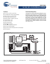
STK11C68
Document Number: 001-50638 Rev. ** Page 2 of 16
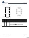
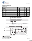
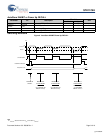
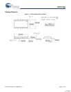
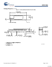
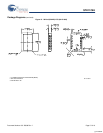
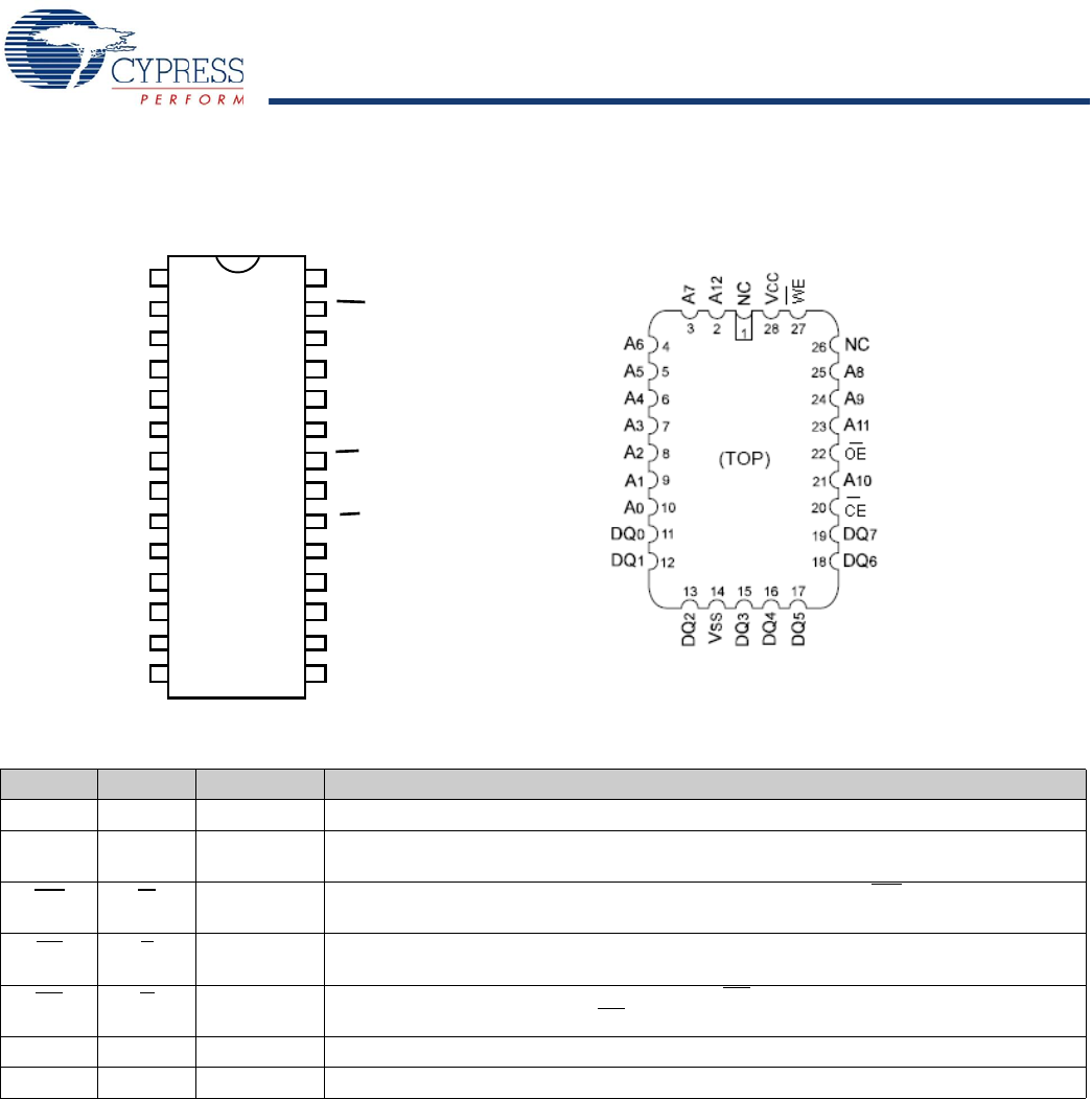
Pin Configurations
Figure 1. Pin Diagram - 28-Pin SOIC/DIP and 28-Pin LLC
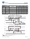
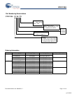
Pin Definitions
Pin Name Alt IO Type Description
A
0
–A
12
Input Address Inputs. Used to select one of the 8,192 bytes of the nvSRAM.
DQ
0
-DQ
7
Input or
Output
Bidirectional Data IO Lines. Used as input or output lines depending on operation.
WE
W
Input Write Enable Input, Active LOW. When the chip is enabled and WE is LOW, data on the
IO pins is written to the specific address location.
CE E
Input Chip Enable Input, Active LOW. When LOW, selects the chip. When HIGH, deselects the
chip.
OE
G
Input Output Enable, Active LOW. The active LOW OE input enables the data output buffers
during read cycles. Deasserting OE
HIGH causes the IO pins to tri-state.
V
SS
Ground Ground for the Device. The device is connected to ground of the system.
V
CC
Power Supply Power Supply Inputs to the Device.
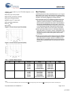
1&
$
$
$
$
$
$
$
$
'4
'4
'4
9
66
9
&&
1&
$
$
$
$
'4
'4
'4
'4
'4
$
:(
2(
&(
723
[+] Feedback