


STK11C68
Document Number: 001-50638 Rev. ** Page 7 of 16
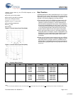
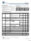
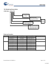
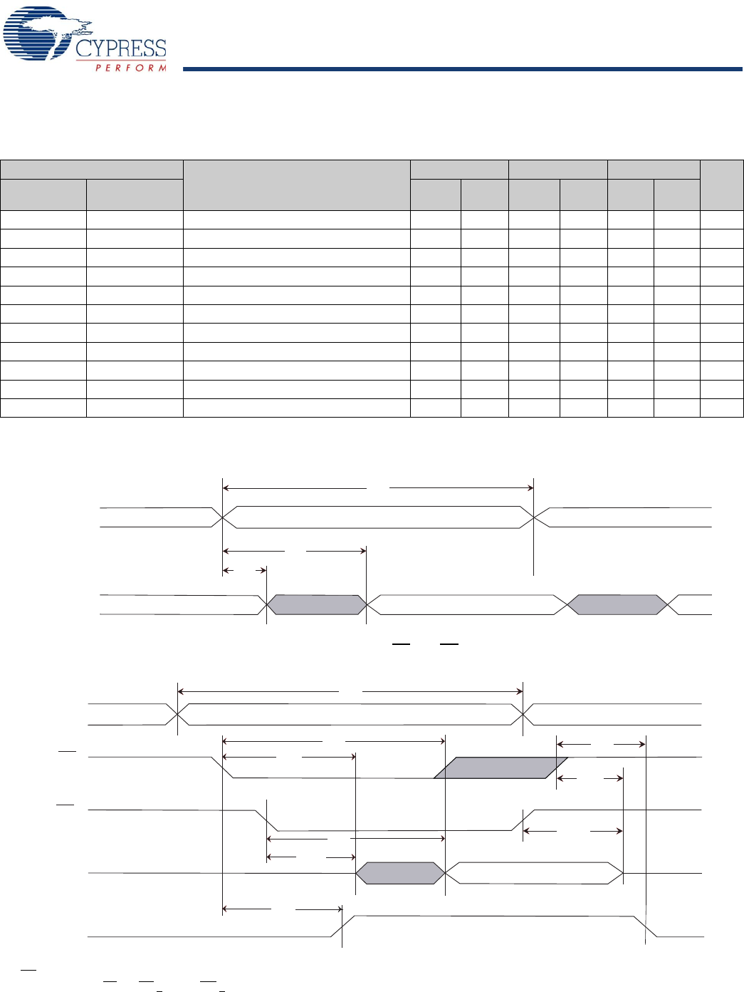
AC Switching Characteristics
SRAM Read Cycle
Parameter
Description
25 ns 35 ns 45 ns
Unit
Min Max Min Max Min Max
Cypress
Parameter
Alt
t
ACE
t
ELQV
Chip Enable Access Time 25 35 45 ns
t
RC
[4]
t
AVAV,
t
ELEH
Read Cycle Time 25 35 45 ns
t
AA
[5]
t
AVQV
Address Access Time 25 35 45 ns
t
DOE
t
GLQV
Output Enable to Data Valid 10 15 20 ns
t
OHA
[5]
t
AXQX
Output Hold After Address Change 5 5 5 ns
t
LZCE
[6]
t
ELQX
Chip Enable to Output Active 5 5 5 ns
t
HZCE
[6]
t
EHQZ
Chip Disable to Output Inactive 10 13 15 ns
t
LZOE
[6]
t
GLQX
Output Enable to Output Active 0 0 0 ns
t
HZOE
[6]
t
GHQZ
Output Disable to Output Inactive 10 13 15 ns
t
PU
[3]
t
ELICCH
Chip Enable to Power Active 0 0 0 ns
t
PD
[3]
t
EHICCL
Chip Disable to Power Standby 25 35 45 ns
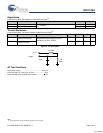
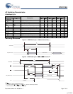
Switching Waveforms
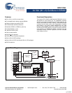
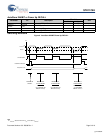
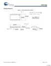
Figure 5. SRAM Read Cycle 1: Address Controlled
[4, 5]
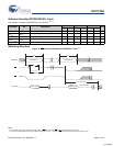
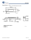
Figure 6. SRAM Read Cycle 2: CE and OE Controlled
[4]
W
5&
W
$$
W
2+$
$''5(66
'4'$7$287
'$7$9$/,'
$''5(66
W
5&
&(
W
$&(
W
/=&(
W
3'
W
+=&(
2(
W
'2(
W
/=2(
W
+=2(
'$7$9$/,'
$&7,9(
67$1'%<
W
38
'4'$7$287
,&&
Notes
4. WE
must be High during SRAM Read cycles.
5. I/O state assumes CE
and OE < V
IL
and WE > V
IH
; device is continuously selected.
6. Measured ±200 mV from steady state output voltage.
[+] Feedback