


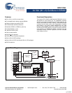
STK11C68
Document Number: 001-50638 Rev. ** Page 4 of 16
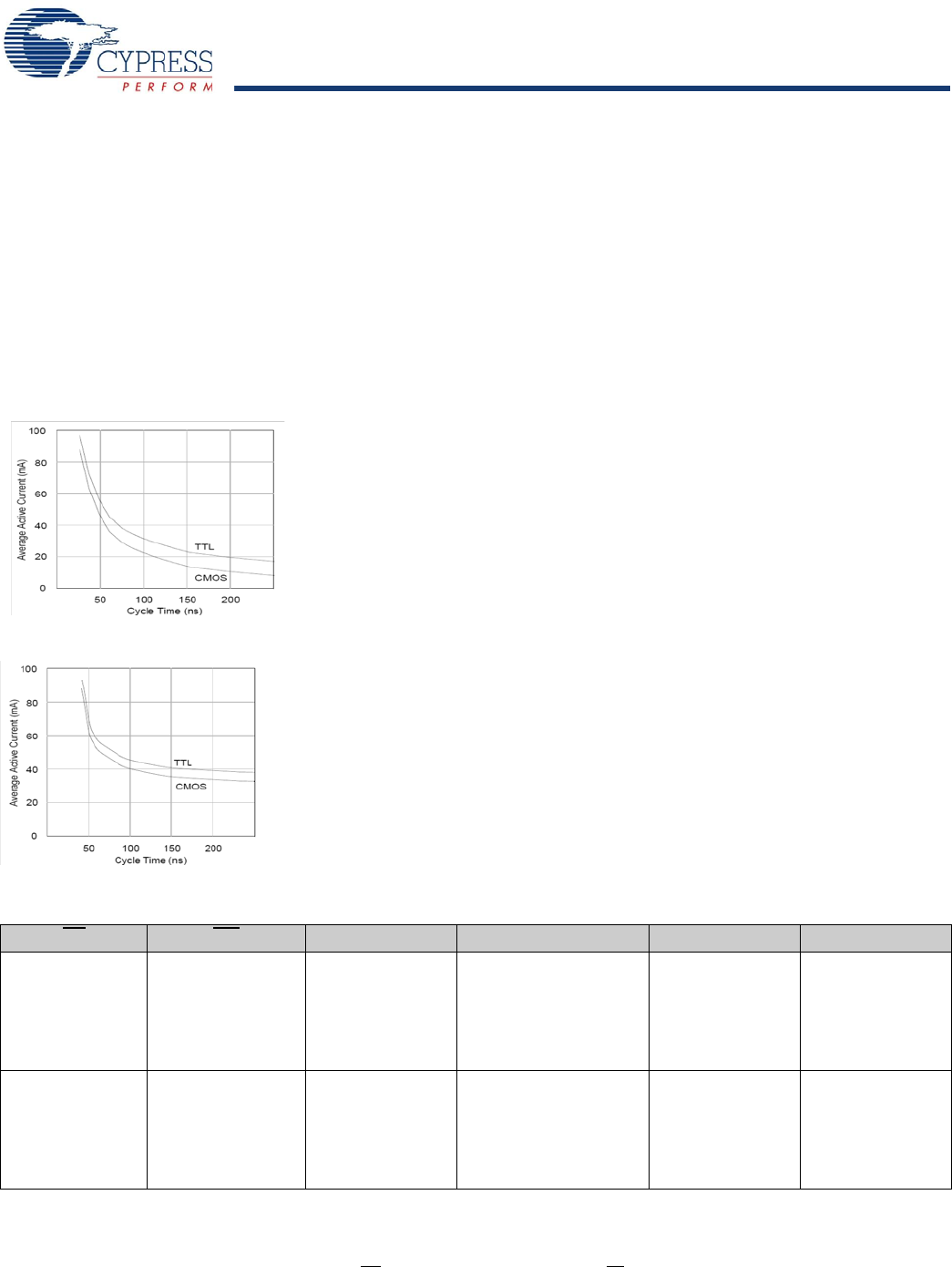
average current drawn by the STK11C68 depends on the
following items:
■
The duty cycle of chip enable
■
The overall cycle rate for accesses
■
The ratio of Reads to Writes
■
CMOS versus TTL input levels
■
The operating temperature
■
The V
CC
level
■
IO loading
Best Practices
nvSRAM products have been used effectively for over 15 years.
While ease of use is one of the product’s main system values,
experience gained working with hundreds of applications has
resulted in the following suggestions as best practices:
■
The nonvolatile cells in an nvSRAM are programmed on the
test floor during final test and quality assurance. Incoming
inspection routines at customer or contract manufacturer’s
sites sometimes reprograms these values. Final NV patterns
are typically repeating patterns of AA, 55, 00, FF, A5, or 5A.
The end product’s firmware should not assume that an NV array
is in a set programmed state. Routines that check memory
content values to determine first time system configuration,
■
cold or warm boot status, and so on must always program a
unique NV pattern (for example, complex 4-byte pattern of 46
E6 49 53 hex or more random bytes) as part of the final system
manufacturing test to ensure these system routines work
consistently.
■
Power up boot firmware routines should rewrite the nvSRAM
into the desired state. While the nvSRAM is shipped in a preset
state, best practice is to again rewrite the nvSRAM into the
desired state as a safeguard against events that might flip the
bit inadvertently (program bugs, incoming inspection routines,
and so on).
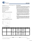
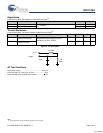
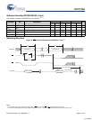
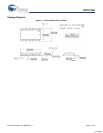
Figure 2. Current Versus Cycle Time (Read)
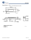
Figure 3. Current Versus Cycle Time (Write)
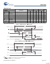
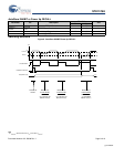
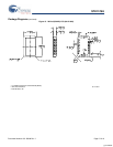
Table 1. Hardware Mode Selection
CE WE A12–A0 Mode IO Notes
L H 0x0000
0x1555
0x0AAA
0x1FFF
0x10F0
0x0F0F
Read SRAM
Read SRAM
Read SRAM
Read SRAM
Read SRAM
Nonvolatile STORE
Output Data
Output Data
Output Data
Output Data
Output Data
Output High Z
[1]
L H 0x0000
0x1555
0x0AAA
0x1FFF
0x10F0
0x0F0E
Read SRAM
Read SRAM
Read SRAM
Read SRAM
Read SRAM
Nonvolatile RECALL
Output Data
Output Data
Output Data
Output Data
Output Data
Output High Z
[1]
Note
1. The six consecutive addresses must be in the order listed. WE
must be high during all six consecutive CE controlled cycles to enable a nonvolatile cycle.
[+] Feedback