


G586SP/G586SP AIO
18
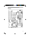
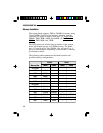
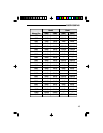
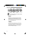
8 Tag Bits 7 Tag Bits
1 Dirty Bit
Cacheable Range
64MB
128MB
256MB
32MB
64MB
128MB
Tag SRAM
8KBx8x1
16/32KBx8x1
32KBx8x1
32KBx8x8
64KBx8x8
128KBx8x8
Cache Size
256KB
512KB
1MB
Data SRAM
Note:
You can change the cacheable range settings by using the
“L2 (WB) Tag Bit Length” option in the Chipset Features
Setup of the Award BIOS utility.
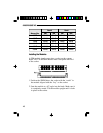
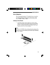
Jumper JP14
Cache Type
Set JP14 pins 1-2 to On if your system board is installed
with asynchronous cache SRAM. Set pins 2-3 to On if the
system board is installed with burst/pipeline burst cache
SRAM. The default is set to pins 2-3 On. If you are install-
ing a cache module, make sure the cache chips have been
removed from the SRAM sockets.
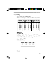
Jumper JP18
L1 Cache Mode
Jumper JP18 is used to select the level 1 cache mode. Set
pins 1-2 to On for write-back cache and pins 2-3 to On for
write-through cache. The default is write-back cache. If you
change the setting of JP18, the “L1 Cache Update Mode”
option in the Chipset Features Setup menu of the BIOS
utility must be changed accordingly.