


EM78P458/459
OTP ROM
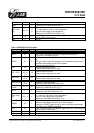
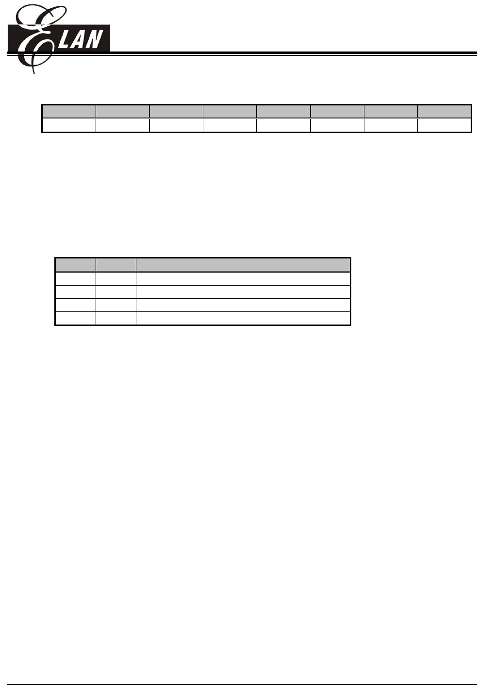
4. R3 (Status Register)
7 6 5 4 3 2 1 0
CMPOUT PS1 PS0 T P Z DC C
• Bit 7 (CMPOUT) the result of the comparator output.
• Bit 6 (PS1) ~ 5 (PS0) Page select bits. PS0~PS1 are used to select a program memory page. When
executing a "JMP", "CALL", or other instructions which cause the program counter to be changed
(e.g. MOV R2, A), PS0~PS1 are loaded into the 11th and 12th bits of the program counter where it
selects one of the available program memory pages. Note that RET (RETL, RETI) instruction does
not change the PS0~PS1 bits. That is, the return will always be to the page from the place where the
subroutine was called, regardless of the current setting of PS0~PS1 bits.
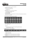
PS1 PS0 Program memory page [Address]
0 0 Page 0 [000-3FF]
0 1 Page 1 [400-7FF]
1 0 Page 2 [800-BFF]
1 1 Page 3 [C00-FFF]
• Bit 4 (T) Time-out bit. Set to 1 by the "SLEP" and "WDTC" commands, or during Power on and reset
to 0 by WDT time-out.
• Bit 3 (P) Power-down bit. Set to 1 during power-on or by a "WDTC" command and reset to 0 by a
"SLEP" command.
• Bit 2 (Z) Zero flag. Set to "1" if the result of an arithmetic or logic operation is zero.
• Bit 1 (DC) Auxiliary carry flag
• Bit 0 (C) Carry flag
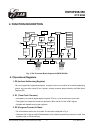
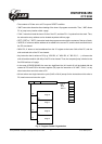
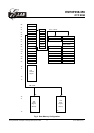
5. R4 (RAM Select Register)
• Bits 0~5 are used to select registers (address: 00~3F) in the indirect address mode.
• Bit 6 is used to select bank 0 or bank 1.
• Bit 7 is a general-purpose read/write bit.
• See the configuration of the data memory in Fig. 4.
6. R5 ~ R6 (Port 5 ~ Port 6)
• R5 and R6 are I/O registers.
7. R7 ~ R8
• All of these are 8-bit general-purpose registers.
This specification is subject to change without prior notice. 07.01.2003 (V1.3)
10