


RTC - 4543 SA/SB
Page - 7 MQ - 252 - 03
7. Description of Operation
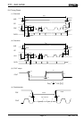
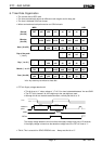
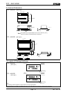
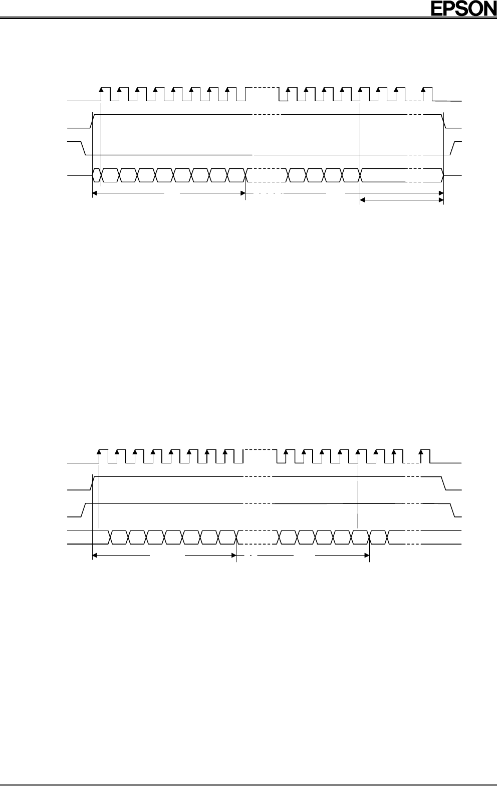
7-1.Data reads
CLK
WR
DATA
FDTs40s20s10s8s4s2s1 y8 y10 y20 y40
CE
y80
1 52
Sec
2 53 54 54+n
Output data does not change
Year
1) When the WR pin is low and the CE pin is high, the RTC enters data output mode.
2) At the first rising edge of the CLK signal, the clock and calendar data are loaded into the shift
register and the LSB of the seconds digits is output from the DATA pin.
3) The remaining seconds, minutes, hour, day of the week, day, month, and year data is shifted out,
in sequence and in synchronization with the rising edge of the CLK signal, so that the data is
output from the DATA pin.
The output data is valid until the rising edge of the 52nd clock pulse; even if more than 52 clock
pulses are input,
the output data does not change.
4) If data is required in less than 52 clock pulses, that part of the data can be gotten by setting the
CE pin low after the necessary number of clock pulses have been output.
Example: If only the data from “seconds” to “day of the week” is needed:
After 28 clock pulses, set the CE pin low in order to get the data from “seconds” to “day of
the week.”
5) When performing successive data read operations, a wait (tRCV) is necessary after the CE pin
is set low.
6) Note that if an update operation (a one-second carry) occurs during a data read operation,
the data that is read will have an error of -1 second.
7) Complete data read operations within tCE (Max.) = 0.9 seconds, as described earlier.
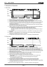
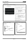
7-2. Data writes
CLK
WR
DATA
0
s40s20s10s8s4s2s1
y8 y10 y20 y40
CE
y80
1 52
( FDT )
2 53 54 54+n
Seconds Year
1) When the WR pin is high and the CE pin is high, the RTC enters data input mode.
2) In this mode, data is input, in succession and in synchronization with the rising edge of the CLK
signal, to the shift register from the DATA pin, starting from the LSB of the seconds digits.
3) The sub-seconds counter is reset between the falling edge of the first clock pulse and the rising
edge of the second clock pulse. In addition, carries to the seconds counter are prohibited at the
falling edge of the first clock pulse.
4) After the last data is input to the shift register at the rising edge of the 52nd clock pulse, the
contents of the shift register are transferred to the timer counter.
5) Note that during a data write operation, 52 bits of data must be input.
•
Correct write-access isn't completed when CE terminal turned into low on a state of less
than 52 bits.
•
If more than 52 bits of data are input, the 53rd and subsequent bits are ignored.
(The first 52 bits of data are valid.)
6) Once the CE pin is set low, the prohibition on carries to the seconds counter is lifted.
Complete data write operations within t
CE
(Max.) = 0.9 seconds, as described earlier.
7) If a data read operation is to be performed immediately after a data write operation, a wait (tRCV)
is necessary after the CE pin is set low.
* Malfunction will result if illegal data is written. Therefore, be certain to write legal data.