


RTC - 4543 SA/SB
Page - 2 MQ - 252 - 03
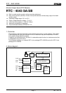
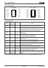
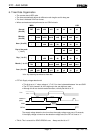
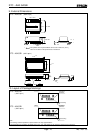
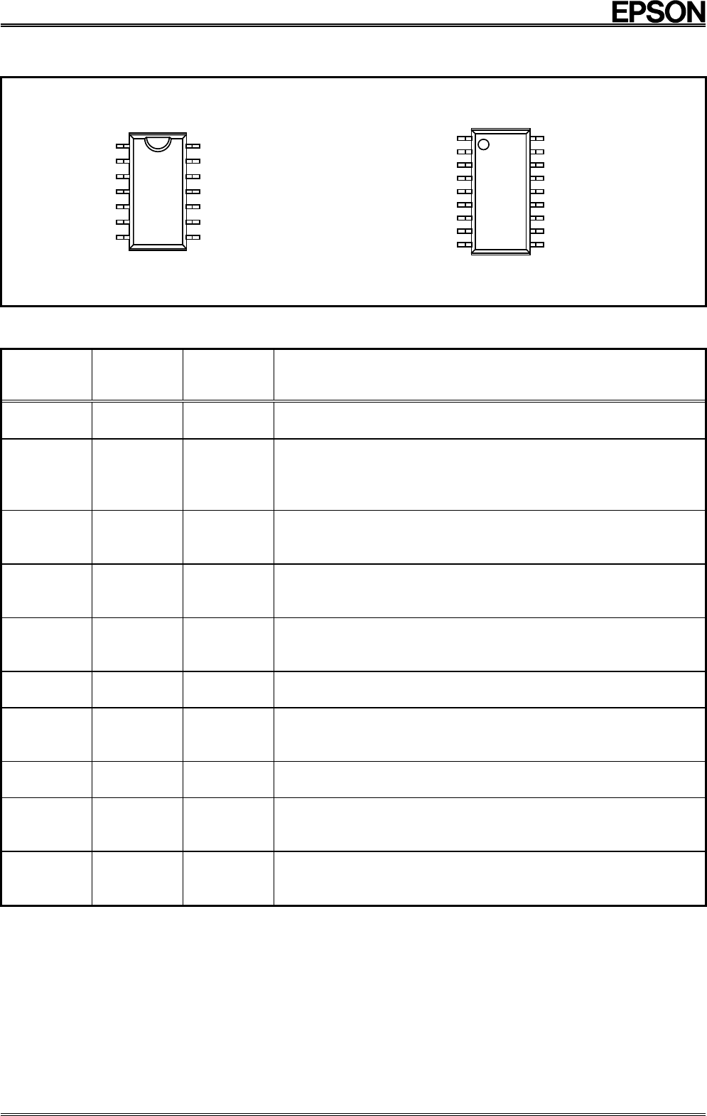
3. Pin Connections
1
78
14
2
3
4
5
6
1
7
14
12
11
10
9
8
13
GND
CLK
WR
FOUT
DATA
CE
DD
V
FOE
N.C
FSEL
N.C
N.C
N.C
N.C
RTC - 4543SA
SOP - 14pin
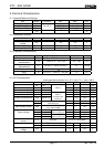
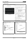
1
910
18
2
3
4
5
6
1
7
9
8
GND
WR
CE
DD
V
FOE
N.C
FSEL
N.C
N.C
17
16
15
14
13
18
12
10
11
N.C
N.C
N.C
N.C
N.C
CLK
DATA
FOUT
N.C
RTC - 4543SB
SOP - 18pin
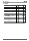
4. Pin Functions
Signal
Pin No.
SOP-14pin
(SOP-18pin)
I/O Function
GND
1
( 9 )
Connects to negative (-) side (ground) of the power supply.
CE
3
( 8 )
Input
Chip enable input pin.
When high,the chip is enabled. When low,the DATA pin goes to
high impedance and the CLK,DATA,and WR pins are not able to
accept input.In addition, when low,the TM bit is cleared.
FSEL
4
( 7 )
Input
Serect the frequency that is output from the FOUT pin.
High : 1 Hz
Low : 32.768 kHz
WR
5
( 6 )
Input
DATA pin input/output switching pin.
High : DATA input (when writing the RTC)
Low : DATA output (when reading the RTC)
FOE
6
( 5 )
Input
When high, the frequency selected by the FSEL pin is output from
the FOUT pin.
When low, the FOUT pin goes to high impedance.
V
DD
9
( 14 )
Connects to positive (+) side of the power supply.
CLK
10
( 12 )
Input
Serial clock input pin.
Data is gotten at the rising edge during a write, and data is output
at the rising edge during a read.
DATA
11
( 11 )
Bi-directional Input/outout pin that is used for writing and reading data.
FOUT
14
( 10 )
Output
Outputs the frequency selected by the FSEL pin. 1 Hz output is
synchronized with the internal one-second signal.
This output is not affected by the CE pin.
N.C.
2,7,8,12,13
( 1,2,3,4,13,
15,16,17,18 )
Although these pins are not connected internally,they should
always be left open in order to obtain the most stable oscillation
possible.
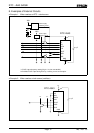
* Always connect a passthrough capacitor of at least 0.1
µ
F as close as possible between V
DD
and GND.