


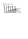
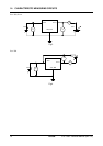
10. PIN DESCRIPTION
6 EPSON S1F77B01 Technical Manual (Rev.1.3)
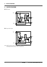
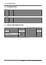
10. PIN DESCRIPTION
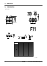
For SOT-23-5
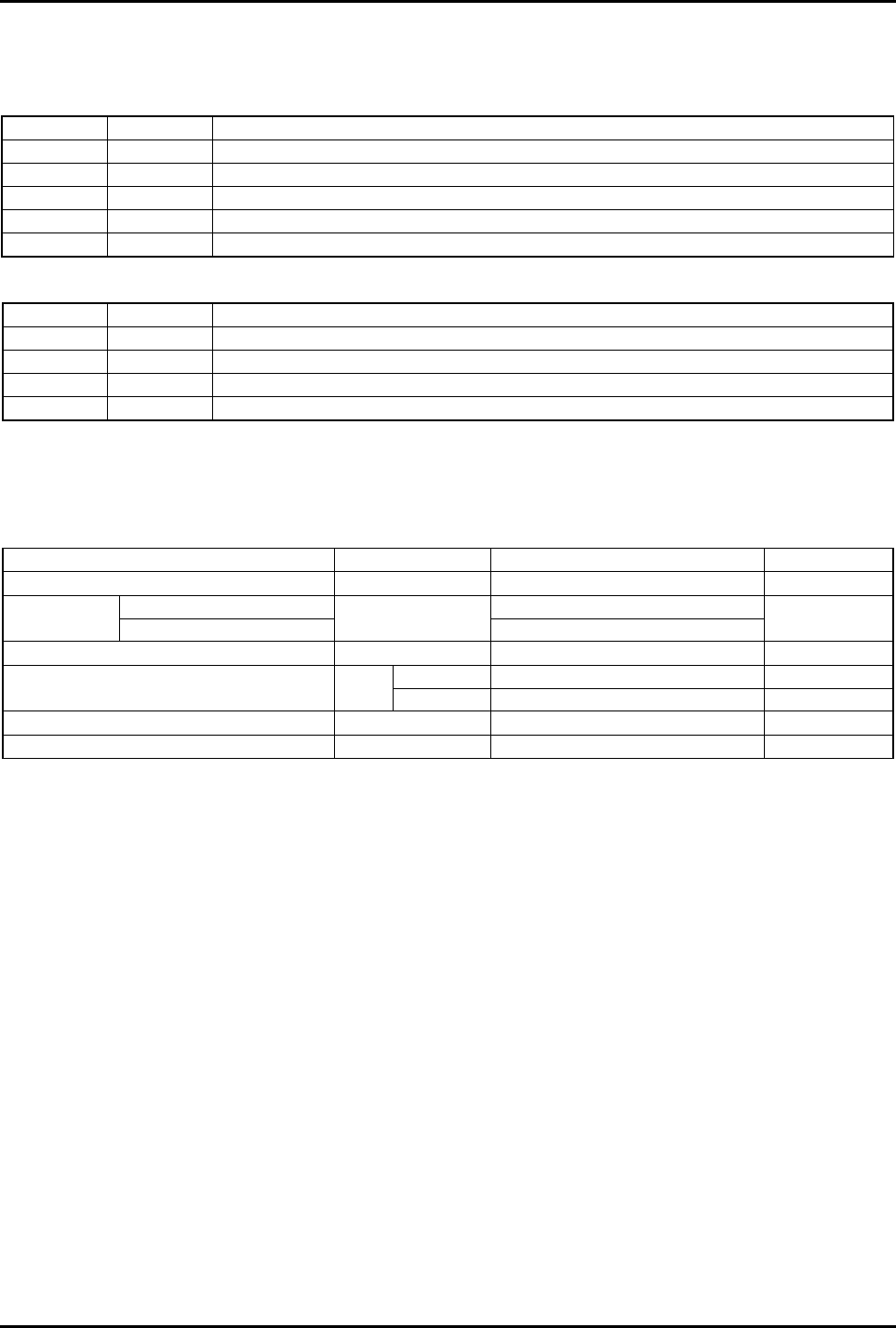
Pin No. Pin Name Function
1 DS Fixed to “LOW”.
2 VSS GND pin.
3 NC No connection
4 VOUT Voltage detection output pin
5 VDD Power input pin
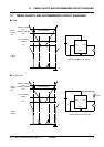
For WCSP
Pin No. Pin Name Function
1 DS Fixed to “LOW”.
2 VSS GND pin.
3 VDD Voltage output pin
4 VOUT Power detection output pin
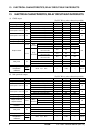
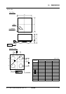
11. ABSOLUTE MAXIMUM RATINGS
(T
a=25°C RL=∞ unless otherwise specified)
Item Symbol Rating Unit
Power voltage VDD-VSS 7.0 V
Nch open drain output VSS-0.3V to 7.0
Output voltage
CMOS output
VOUT
VSS-0.3V to VDD+0.3V
V
Output current IOUT 20 mA
SOT23 300 mW
Allowable dissipation PD
WCSP 100 mW
Guaranteed operating temperature range Topr -40 to +85 °C
Storage temperature range Tstg -40 to +125 °C
Note: To stabilize the IC, insert the decoupling capacitor between V
DD and VSS.