


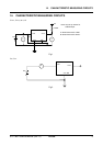
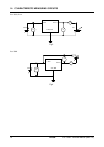
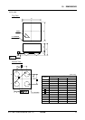
14. CHARACTERISTIC MEASURING CIRCUITS
S1F77B01 Technical Manual (Rev.1.3) EPSON 11
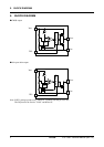
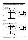
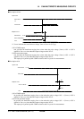
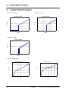
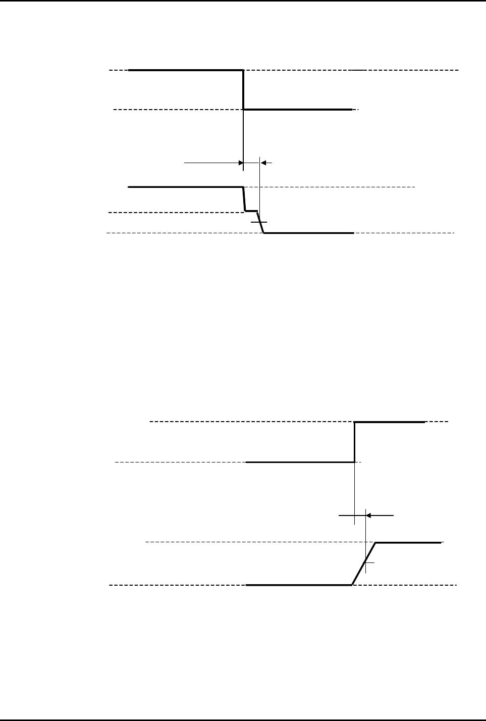
zDescription of tPHL
*3: V
DET+ indicates the actual release voltage. VDET+=VDET-×1.05 (Typ.)
(1) For CMOS output
tPHL provides the timeframe ranging from a time when the pulse voltage (VDET+)+1.0V → 0.9V is
applied to V
DD, to a time when the output voltage reaches VDD/2.
(2) Nch open drain output
tPHL provides the timeframe ranging from a time when the pulse voltage (VDET+)+1.0V → 0.9V is
applied to V
DD, to a time when the output voltage reaches VDD/2.
The output pin is pulled up with 470kΩ resistance and V
DD power for measurement.
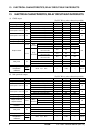
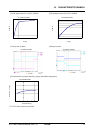
zDescription of
td
(1) For CMOS output
td provides the timeframe ranging from a time when the pulse voltage 0.9V → (VDET+)+1.0V is
applied to V
DD, to a time when the output voltage reaches VDD/2.
(2) For Nch open drain output
td provides the timeframe ranging from a time when the pulse voltage 0.9V → (VDET+)+1.0V is
applied to V
DD, to a time when the output voltage reaches VDD/2.
The output pin is pulled up with 470kΩ resistance and V
DD power for measurement.
50%
tPHL
VDD=0.9V
Input: VDD
Output:
VOUT
VOUT=VDD(0.9V)
V
SS
VDD=VDET+ +1.0V
VDD=VDET+ +1.0V
*3
50%
VDD=VDET+ +1.0V
V
DD=0.9V
Input: V
DD
Output:
VOUT
VOUT= 100 %
V
SS
td