


7.4 Electrical Requirements
C156-E228-02EN 7-11
7.4 Electrical Requirements
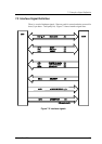
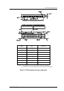
7.4.1 SCSI interface
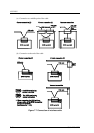
(1) Driver and receiver
For the interface signal driver, an open-collector or tri-state buffer circuit that
satisfies the following output characteristics is used. All signals are negative logic
(true = "L").
The receiver and non-driver of the SCSI device under the power-on state should
satisfy the following input characteristics on each signal.
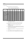
Output characteristics
V
OL
= 0.0 to 0.50 VDC (@ I
OL
= 48 mA)
V
OH
= 2.5 to 5.25 VDC
Input characteristics
V
IL
= 0.0 to 0.80 VDC
I
IL
= –0.4 to 0.0 mA (@ V
I
= 0.5 VDC)
V
IH
= 2.0 to 5.25 VDC
I
IH
= 0.0 to 0.1 mA (@ V
I
= 2.7 VDC)
Input hysteresis = 0.2 VDC min.
Input capacitance = 25
P
F max.
Note: The SCSI device under the power-off state should satisfy the
characteristics of I
IL
and I
IH
.
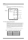
Recommended circuit
Driver: MB463 (Fujitsu) or SN7438 (TI) (Open-collector NAND gate)
Receiver: SN74LS240 or SN74LS19 (TI) (Schmitt trigger input inverter)