


C141-E099-01EN 5 - 3
5.1.2 Signal assignment on the connector
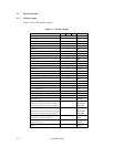
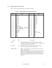
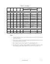
Table 5.2 shows the signal assignment on the interface connector.
Table 5.2 Signal assignment on the interface connector
Pin No. Signal Pin No. Signal
1
3
5
7
9
11
13
15
17
19
21
23
25
27
29
31
33
35
37
39
RESET–
DATA7
DATA6
DATA5
DATA4
DATA3
DATA2
DATA1
DATA0
GND
DMARQ
DIOW–, STOP
DIOR–, HDMARDY–, HSTROBE
IORDY, DDMARDY–,
DSTROBE
DMACK–
INTRQ
DA1
DA0
CS0–
DASP–
2
4
6
8
10
12
14
16
18
20
22
24
26
28
30
32
34
36
38
40
GND
DATA8
DATA9
DATA10
DATA11
DATA12
DATA13
DATA14
DATA15
(KEY)
GND
GND
GND
CSEL
GND
reserved
PDIAG–, CBLID–
DA2
CS1–
GND
[signal] [I/O] [Description]
RESET– I Reset signal from the host. This signal is low active and is
asserted for a minimum of 25 µs during power on. The device has
a 10 kΩ pull-up resistor on this signal.
DATA 0-15 I/O Sixteen-bit bi-directional data bus between the host and the
device. These signals are used for data transfer
DIOW–, STOP I DIOW– is the strobe signal asserted by the host to write device
registers or the data port.
DIOW– shall be negated by the host prior to initiation of an Ultra
DMA burst. STOP shall be negated by the host before data is
transferred in an Ultra DMA burst. Assertion of STOP by the host
during an Ultra DMA burst signals the termination of the Ultra
DMA burst.