


Contents
Contents
1 Product Overview ............................................................................................................5
1.1 Introduction ...........................................................................................................5
1.2 Related Documents...............................................................................................5
1.3 Product Contents ..................................................................................................6
1.4 Proof-of-Concept Board Features..........................................................................6
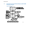
1.5 Intel® ECX Form Factor POC Board Based on Intel® 915GM Chipset Block
Diagram ................................................................................................................8
2 Installation Guide for POC Board ...................................................................................9
2.1 Before You Begin..................................................................................................9
2.2 Setting up the Intel® ECX POC Board...................................................................9
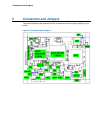
3 Connectors and Jumpers..............................................................................................14
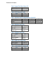
3.1 List of Jumpers....................................................................................................15
3.2 List of Connectors ...............................................................................................17
Figures
Figure 1. Block Diagram ....................................................................................................8
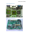
Figure 2. Assembly board, Top View................................................................................11
Figure 3. Assembly board, Bottom View...........................................................................11
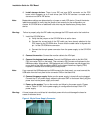
Figure 4. 20-pin Power Supply Connector........................................................................12
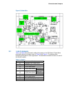
Figure 5. Connectors and Jumpers ..................................................................................14
Figure 6. Solder Side.......................................................................................................15
Tables
Table 1. Related Documents..............................................................................................5
Table 2. Additional Hardware.............................................................................................9
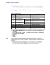
Table 3. Jumper Settings.................................................................................................10
Table 4. Jumpers.............................................................................................................15
Table 5. Compact Flash Power Select (JP1)...................................................................16
Table 6. LVDS Voltage select (JP2)................................................................................16
Table 7. COM1 Mode Select for RS-232/422/485 (JP3/JP6/JP7) ....................................16
Table 8. COM1 Mode Select (JP4)...................................................................................16
Table 9. COM2 Mode Select (JP5)...................................................................................16
Table 10. CMOS Clear Jumper (JP8)...............................................................................16
Table 11. Audio Output Select Jumper (JP9)....................................................................16
Table 12. Connectors ......................................................................................................17
Table 13. Digital I/O Connector (CN1)..............................................................................17
Table 14. Front Panel Bezel Connector (CN2) .................................................................17
Table 15. Primary IDE Hard Drive Connector (CN3).........................................................18
Table 16. Parallel Port Connector (CN4)..........................................................................18
Table 17. USB Port2 & Port3 Connector (CN5)................................................................19