A Detailed Look Inside the Intel
®
NetBurst
™
Micro-Architecture of the Intel Pentium
®
4 Processor
Page 15
Port 3. Port 3 supports the dispatch of one store address operation per cycle.
Thus the total issue bandwidth can range from zero to six µops per cycle. Each pipeline contains several execution
units. The µops are dispatched to the pipeline that corresponds to its type of operation. For example, an integer
arithmetic logic unit and the floating-point execution units (adder, multiplier, and divider) share a pipeline.
Caches
The Intel NetBurst micro-architecture can support up to three levels of on-chip cache. Only two levels of on-chip
caches are implemented in the Pentium 4 processor, which is a product for the desktop environment. The level
nearest to the execution core of the processor, the first level, contains separate caches for instructions and data: a
first-level data cache and the trace cache, which is an advanced first-level instruction cache. All other levels of
caches are shared. The levels in the cache hierarchy are not inclusive, that is, the fact that a line is in level i does not
imply that it is also in level i+1. All caches use a pseudo-LRU (least recently used) replacement algorithm. Table 1
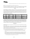
provides the parameters for all cache levels.
Table 1 Pentium 4 Processor Cache Parameters
Level Capacity Associativity
(ways)
Line Size
(bytes)
Access Latency (clocks),
Integer/floating-point
Write Update Policy
First 8KB 4 64 2/6 write through
TC 12K µops N/A N/A N/A N/A
Second 256KB 8 128 7/7 write back
A second-level cache miss initiates a transaction across the system bus interface to the memory sub-system. The
system bus interface supports using a scalable bus clock and achieves an effective speed that quadruples the speed of
the scalable bus clock. It takes on the order of 12 processor cycles to get to the bus and back within the processor,
and 6-12 bus cycles to access memory if there is no bus congestion. Each bus cycle equals several processor cycles.
The ratio of processor clock speed to the scalable bus clock speed is referred to as bus ratio. For example, one bus
cycle for a 100 MHz bus is equal to 15 processor cycles on a 1.50 GHz processor. Since the speed of the bus is
implementation- dependent, consult the specifications of a given system for further details.
Data Prefetch
The Pentium 4 processor has two mechanisms for prefetching data: a software-controlled prefetch and an automatic
hardware prefetch.
Software-controlled prefetch is enabled using the four prefetch instructions introduced with Streaming SIMD
Extensions (SSE) instructions. These instructions are hints to bring a cache line of data into the desired levels of the
cache hierarchy. The software-controlled prefetch is not intended for prefetching code. Using it can incur significant
penalties on a multiprocessor system where code is shared.
Software-controlled data prefetch can provide optimal benefits in some situations, and may not be beneficial in other
situations. The situations that can benefit from software-controlled data prefetch are the following:
§ when the pattern of memory access operations in software allows the programmer to hide memory latency
§ when a reasonable choice can be made of how many cache lines to fetch ahead of the current line being
executed
§ when an appropriate choice is made for the type of prefetch used. The four types of prefetches have different
behaviors, both in terms of which cache levels are updated and the performance characteristics for a given
processor implementation. For instance, a processor may implement the non-temporal prefetch by only
returning data to the cache level closest to the processor core. This approach can have the following effects:
a) minimizing disturbance of temporal data in other cache levels


