– 95 –
APPENDIX D
PCI-1712/1712L User’s Manual
Advantech Co., Ltd.
www.advantech.com
.ddAesaB 51 41 31 21 11 01 9 8 7 6 5 4 3 2 1 0
81
W
0retnuocA/D
7D 6D 5D 4D 3D 2D 1D 0D
R
0retnuocA/D
7D 6D 5D 4D 3D 2D 1D 0D
A1
W
1retnuocD/A
7D 6D 5D 4D 3D 2D 1D 0D
R
1retnuocD/A
7D 6D 5D 4D 3D 2D 1D 0D
C1
W
2retnuocAMD
7D 6D 5D 4D 3D 2D 1D 0D
R
2retnuocAMD
7D 6D 5D 4D 3D 2D 1D 0D
E1
W
lortnocretnuoC
7D 6D 5D 4D 3D 2D 1D 0D
R
lortnocretnuoC
7D 6D 5D 4D 3D 2D 1D 0D
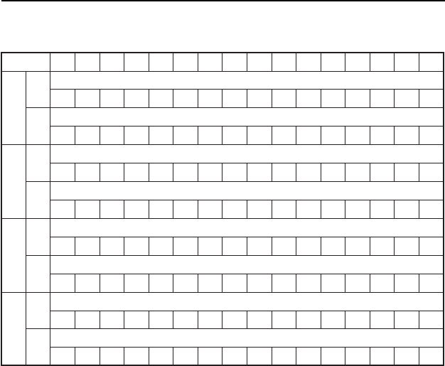
D.13 82C54 counter chip 1 — Write/Read BASE+18 to 1E
Table D-14: Register for 82C54 counter chip 1
This counter chip 82C54 includes three counters for general purpose.
These three counters are identical. They can do event counting, rate
generation, one shot, frequency measurement and pulse width
measurement. Please refer to chapter 5.3 for more details about the
principles of operation. In order to explain the functions of three
counters clearly, we adopt a naming rule to designate the counter
number. For example, as you will see in the subsequent sections, there
are many registers with names like Cn0, CPn, CQn, etc. Note that the
“n” in these register names represents the counter number that is
concerned.


