


– 57 –
Chapter 6
PCI-1712/1712L User’s Manual
Advantech Co., Ltd.
www.advantech.com
mode. Adjust the gain until the AI0’s value converges between
0 and 1.
7. Repeat steps 4 to 6 several times.
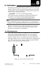
6.3 D/A Calibration
You can select an on-board +5V or +10V internal reference voltage or
an external voltage as your analog output reference voltage. If you
use an external reference, connect the reference voltage within the
±10V range to the reference input of the D/A output channel you want
to calibrate. Then adjust the gain value, unipolar offset voltage, bipolar
offset voltage, respectively, of D/A channels 0 and 1 with the associ-
ated register (BASE+2C).
Note:
✎ A precision voltmeter is recommended to calibrate the D/A outputs.
The auto-calibration program AutoCali.EXE helps you finish the D/A
calibration procedure automatically. In order to get the maximum
possible accuracy of the D/A channels, you need to calibrate the A/D
channels first. Although the procedure is not necessary, the following
calibration steps are provided below for your reference in case you
want to implement the calibration yourself:
1. Calibrate the A/D channels first.
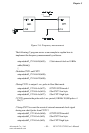
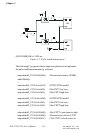
2. Set PCI-1712 in calibration mode. AI4 is connected to AO0 and
AI6 is connected to AO1. (Write “1” to the bit, AIO_CAL, on
register BASE+6 bit7)
3. Set the unipolar output range of both AO0 and AO1 the same as
the internal or external reference voltage range, either 0 to 5V or
0 to 10 V.
4. Set the output value of the AOn (where n=0 or 1) data register at
(BASE+0x0C) as 0x0ffe and output to AOn.
5. Adjust the associated gain register (BASE+0x0C) until the AOn
output value reads AI4+2n equals 0x0ffe.
6. Set the output value of the AOn data register (BASE+0x0C) as
0x0001 and output to AOn.
7. Adjust the associated unipolar offset register (BASE+0x2C) until