


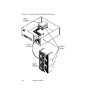
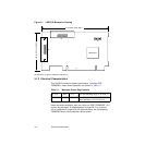
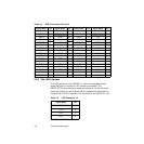
3-4 Technical Specifications
Note: The + 3.3 V pins are tied together and decoupled with high
frequency bypass capacitors to ground. No current from
these 3.3 V pins is used on the board. The PCI portion of
the LSI53C875J chip is powered from the 3 V/5 V pins.
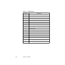
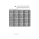
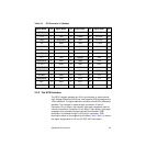
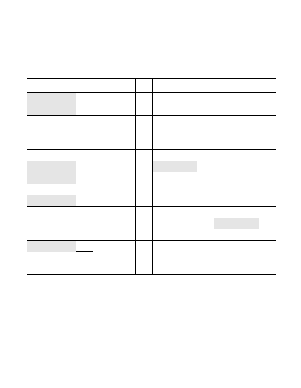
Table 3.2 PCI Connector JI (Top)
Signal Name
1
Pin Signal Name
1
Pin Signal Name
1
Pin Signal Name
1
Pin
-12 V 1 GND 17 C_BE2/ 33 GND 49
TCK 2 REQ/ 18 GND 34 KEYWAY 50
GND 3 3 V/5 V 19 IRDY/ 35 KEYWAY 51
TDO 4 AD31 20 +3.3 V 36 AD08 52
+5 V 5 AD29 21 DEVSEL/ 37 AD07 53
+5 V 6 GND 22 GND 38 +3.3 V 54
INTB/ 7 AD27 23 LOCK/ 39 AD05 55
INTD/ 8 AD25 24 PERR/ 40 AD03 56
GND (PRSNT1/) 9 +3.3 V 25 +3.3 V 41 GND 57
RESERVED 10 C_BE3/ 26 SERR/ 42 AD01 58
GND (PRSNT2/) 11 AD23 27 +3.3 V 43 3 V/5 V 59
KEYWAY 12 GND 28 C_BE1/ 44
ACK64/ 60
KEYWAY 13 AD21 29 AD14 45 +5 V 61
RESERVED 14 AD19 30 GND 46 +5 V 62
GND 15 +3.3 V 31 AD12 47
CLK 16 AD17 32 AD10 48
1. Shaded signals are not connected.