PCI-QUAD-AC5 User's Guide Functional Details
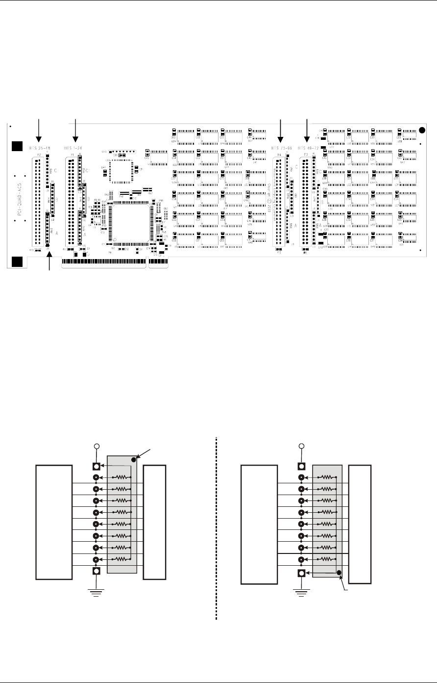
The PCI-QUAD-AC5 board has open locations where you can install a 2.2 K ohm, eight-resistor single
inline package (SIP) resistor network for each port. Each of the four port locations is identified by the bit
range — the First Port connector (P1) is labeled
Bits 1 to 24, the Second Port connector (P2) is labeled
Bits 25 to 48, the Third Port connector (P3) is labeled
Bits 49 to 72, and the Fourth Port connector (P4)
is labeled
Bits 73 to 96. Pull-up/pull-down SIP locations (3 per port) are labeled A, B and C, and are
adjacent to each port. Refer to Figure 4-4.
First Port Fourth Port
SIP locations
A, B, C
3
er
ort
Third Port Second Port
Figure 4-4. PCI-QUAD-AC5 layout and SIP locations
When installed, the SIP establishes either a high or low logic level at each of the eight
I/O lines on the port. At each board location, A, B, and C, there are 10 holes in a line. The hole on one
end is marked "HI" and is connected to +5V. The other end is marked "LO" and is connected to GND.
The eight holes in the middle connect to the eight lines of the port, A, B or C.
To pull-up lines, orient the SIP with the common pin (dot) toward the HI end; to pull-down, install the
resistor with the common pin in the LO end.
Figure 4-5
Figure 4-5. Pull-up and pull-down resistor SIP schematic
shows a schematic of an SIP installed in both the pull-up and pull-down positions.
2.2 K SIP installed for pull-up
2.2 K SIP
Dot indicates the
common line
+5 VDC
HI
LO
(GND)
n7
User Connector
Digital I/O Lines
n5
n4
n3
n2
n1
n0
n6
COM
Digital
I/O Port
n = A, B, or C
+5 VDC
2.2 K SIP installed for pull-down
2.2 K SIP
Dot indicates the
common line
HI
LO
(GND)
n7
User Connector
Digital I/O Lines
n5
n4
n3
n2
n1
n0
n6
COM
Digital
I/O Port
n = A, B, or C
We recommend using 2.2KΩ SIPs (MCC part number SP-K2.29C). Use a different value only if
necessary.
4-2


