Chapter 2 Hardware Overview
© National Instruments Corporation 2-5 NI 5620 User Manual
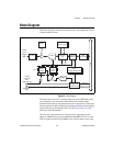
Block Diagram
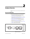
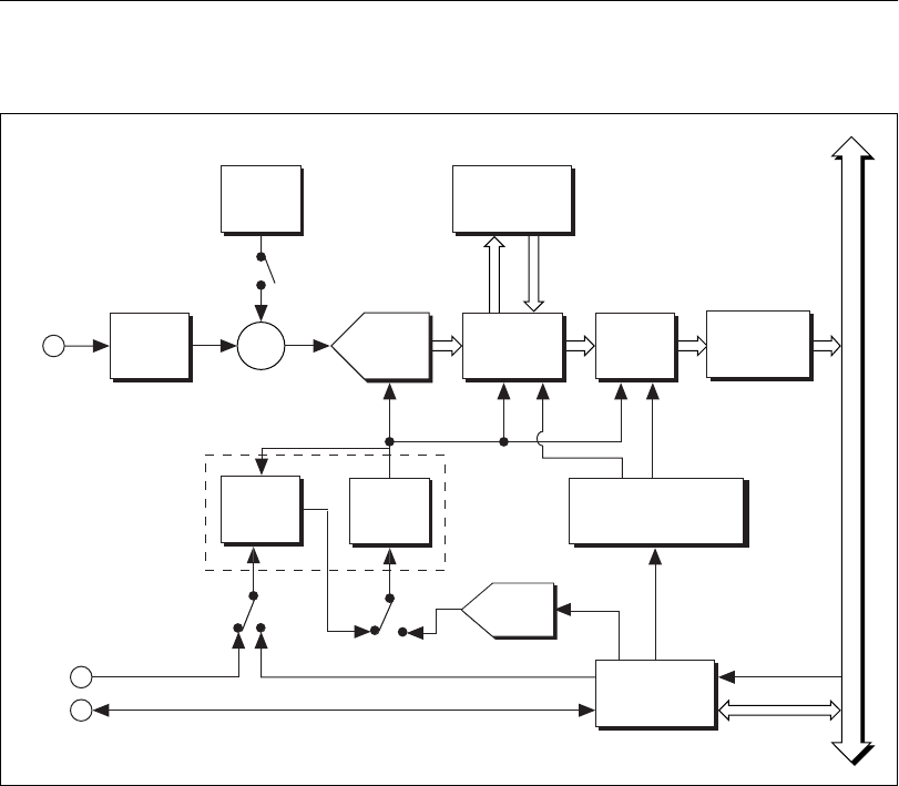
This block diagram isintended for advanced users. Anexplanation of some
of these features follows.
Figure 2-3. Block Diagram
The digital downconverter is a digital signal processor (DSP) that allows
you to digitally zoom in on data, which reduces the amount of data
transferred into memory and speeds up the rate of data transfer. The digital
downconverterdoes this by frequency-translating, filtering, and decimating
signals after they go through the ADC. See the Incorporating the DDC
section for more information.
The PLL uses a phase dectetor to synchronize the acquisition clock to
either a 10 MHz reference clock supplied through REF CLK IN or to the
CLK 10 signal from the PXI backplane. You can also choose to leave the
TIO
(Timing and Control)
Digital
Downconverter
Voltage
Controlled
Oscillator
P
X
I
Data Path
Logic
Onboard
Memory
Filter
MITE
(PXI Interface)
ADC
Dither
+
Analog
Input
(INPUT)
Trigger and
Clock Routing
10 MHz
Reference
Input
(REF CLK IN)
EXT TRIG
(PFI)
External Trigger
PXI Trigger
CLK 10
Phase
Detector
CalDAC
PLL


