


Philips Semiconductors Product specification
Logic level TOPFET PIP3107-D
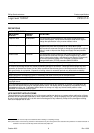
OUTPUT CHARACTERISTICS
Limits are for -40˚C ≤ T
mb
≤ 150˚C; typicals are for T
mb
= 25 ˚C unless otherwise specified
SYMBOL PARAMETER CONDITIONS MIN. TYP. MAX. UNIT
Off-state V
IS
= 0 V
V
(CL)DSS
Drain-source clamping voltage I
D
= 10 mA 50 - - V
I
DM
= 2 A; t
p
≤ 300 µs; δ ≤ 0.01 50 60 70 V
I
DSS
Drain source leakage current V
DS
= 40 V - - 100 µA
T
mb
= 25 ˚C - 0.1 10 µA
On-state I
DM
= 6 A; t
p
≤ 300 µs; δ ≤ 0.01
R
DS(ON)
Drain-source resistance V
IS
≥ 4.4 V - - 95 mΩ
T
mb
= 25 ˚C - 36 50 mΩ
V
IS
≥ 4 V - - 100 mΩ
T
mb
= 25 ˚C - 39 55 mΩ
OVERLOAD CHARACTERISTICS
-40˚C ≤ T
mb
≤ 150˚C unless otherwise specified.
SYMBOL PARAMETER CONDITIONS MIN. TYP. MAX. UNIT
Short circuit load V
DS
= 13 V
I
D
Drain current limiting V
IS
= 5 V; T
mb
= 25˚C 16 24 32 A
4.4 V ≤ V
IS
≤ 5.5 V 12 - 36 A
4 V ≤ V
IS
≤ 5.5 V 8 - 36 A
Overload protection V
IS
= 5 V;T
mb
= 25˚C
P
D(TO)
Overload power threshold device trips if P
D
> P
D(TO)
40 120 160 W
T
DSC
Characteristic time which determines trip time
1
200 350 600 µs
Overtemperature protection
T
j(TO)
Threshold junction 150 170 - ˚C
temperature
2
1 Trip time t
d sc
varies with overload dissipation P
D
according to the formula t
d sc
≈ T
DSC
/ ln[ P
D
/ P
D(TO)
].
2 This is independent of the dV/dt of input voltage V
IS
.
October 2001 3 Rev 1.000