


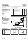

Philips Semiconductors Product specification
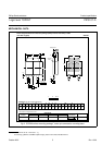
Logic level TOPFET PIP3107-D
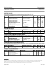
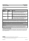
INPUT CHARACTERISTICS
The supply for the logic and overload protection is taken from the input.
Limits are for -40˚C ≤ T
mb
≤ 150˚C; typicals are for T
mb
= 25˚C unless otherwise specified
SYMBOL PARAMETER CONDITIONS MIN. TYP. MAX. UNIT
V
IS(TO)
Input threshold voltage V
DS
= 5 V; I
D
= 1 mA 0.6 - 2.4 V
T
mb
= 25˚C 1.1 1.6 2.1 V
I
IS
Input supply current normal operation; V
IS
= 5 V 100 220 400 µA
V
IS
= 4 V 80 195 330 µA
I
ISL
Input supply current protection latched; V
IS
= 5 V 200 400 650 µA
V
IS
= 3 V 130 250 430 µA
V
ISR
Protection reset voltage
1
reset time t
r
≥ 100 µs 1.5 2 2.9 V
t
lr
Latch reset time V
IS1
= 5 V, V
IS2
< 1 V 10 40 100 µs
V
(CL)IS
Input clamping voltage I
I
= 1.5 mA 5.5 - 8.5 V
R
IG
Input series resistance
2
T
mb
= 25˚C - 33 - kΩ
to gate of power MOSFET
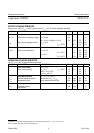
SWITCHING CHARACTERISTICS
T
mb
= 25 ˚C; V
DD
= 13 V; resistive load R
L
= 4 Ω. Refer to waveform figure and test circuit.
SYMBOL PARAMETER CONDITIONS MIN. TYP. MAX. UNIT
t
d on
Turn-on delay time V
IS
= 5 V - 15 30 µs
t
r
Rise time - 30 60 µs
t
d off
Turn-off delay time V
IS
= 0 V - 70 140 µs
t
f
Fall time - 35 70 µs
1 The input voltage below which the overload protection circuits will be reset.
2 Not directly measureable from device terminals.
October 2001 4 Rev 1.000