


Philips Semiconductors Product data
CBTD3306Dual bus switch with level shifting
2
2001 Nov 08 853-2305 27313
FEATURES
• Designed to be used in 5 V to 3.3 V level shifting applications with
internal diode.
• 5 Ω switch connection between two ports
• TTL-compatible input levels
• Package options include plastic small outline (SO) and
thin shrink small outline (TSSOP)
• Latch-up protection exceeds 100 mA per JESD78
• ESD protection exceeds 2000 V HBM per JESD22-A114 and
1000 V CDM per JESD22-C101
DESCRIPTION
The CBTD3306 Dual FET Bus Switch features independent line
switches. Each switch is disabled with the associated Output Enable
(OE
) input is high.
The CBTD3306 is characterized for operation from –40 to +85 °C.
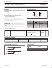
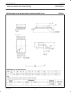
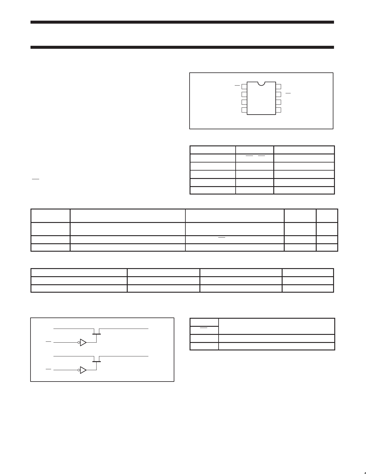
PIN CONFIGURATION
1
2
3
45
6
7
8
1OE
1A
1B
GND
V
CC
2OE
2B
2A
SA00535
PIN DESCRIPTION
PIN NUMBER SYMBOL NAME AND FUNCTION
1, 7 1OE, 2OE Output enable
2, 5 1A, 2A A port inputs
3, 6 1B, 2B B port outputs
4 GND Ground (0V)
8 V
CC
Positive supply voltage
QUICK REFERENCE DATA
SYMBOL PARAMETER
CONDITIONS
T
amb
= 25 °C; GND = 0 V
TYPICAL UNIT
t
PLH
t
PHL
Propagation delay
A to B or B to A
C
L
= 50 pF; V
CC
= +5.0 V ±0.5 V 0.25 (MAX) ns
C
IO(OFF)
Pin capacitance (OFF state) V
O
= 3 V or 0; OE = V
CC
6.50 pF
I
CC
Quiescent supply current V
CC
= 5.5 V; I
O
= 0, V
I
= V
CC
or GND 3 µA
ORDERING INFORMATION
PACKAGES TEMPERATURE RANGE ORDER CODE DWG NUMBER
8-pin plastic SO –40 to 85 °C CBTD3306D SOT96-1
8-pin plastic TSSOP –40 to 85 °C CBTD3306PW SOT530-1
Standard packing quantities and other packaging data is available at www.philipslogic.com/packaging.
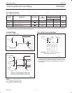
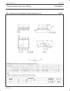
LOGIC DIAGRAM (positive logic)
2
1A
3
1B
SA00534
1
1OE
5
2A
6
2B
7
2OE
FUNCTION TABLE
INPUT
FUNCTION
OE
FUNCTION
L A port = B port
H Disconnect