


Philips Semiconductors Product data
CBTD3306Dual bus switch with level shifting
2001 Nov 08
4
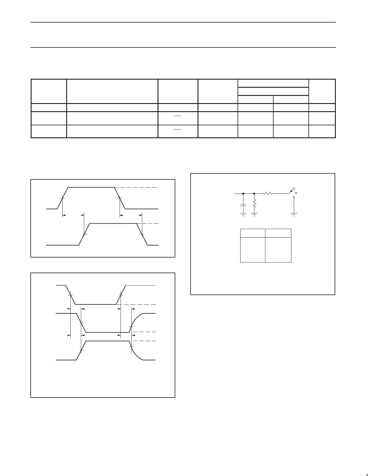
AC CHARACTERISTICS
T
amb
= –40 to +85 °C; C
L
= 50 pF
TO
LIMITS
SYMBOL PARAMETER FROM (INPUT)
TO
(OUTPUT)
V
CC
= +5.0 V ±0.5 V
UNIT
(OUTPUT)
MIN MAX
t
pd
Propagation delay
1
A or B B or A — 0.25 ns
t
en
Output enable time
to High and Low level
OE A or B 1 5 ns
t
dis
Output disable time
from High and Low level
OE A or B 1 4.9 ns
NOTE:
1. The propagation delay is the calculated RC time constant of the typical on-state resistance of the switch and the specified load capacitance,
when driven by an ideal voltage source (zero output impedance).
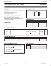
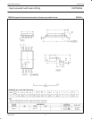
AC WAVEFORMS
V
M
= 1.5 V, V
IN
= GND to 3.0 V
INPUT
1.5 V
OUTPUT
t
PLH
t
PHL
SA00028
1.5 V
1.5 V 1.5 V
3 V
0 V
V
OH
V
OL
Waveform 1. Input to Output Propagation Delays
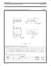
Output Control
(Low-level
enabling )
1.5 V
t
PZH
t
PHZ
V
OH
V
OL
t
PZL
t
PLZ
3.5 V
0 V
V
OL
+ 0.3 V
V
OH
– 0.3 V
SA00029
1.5 V
1.5 V 1.5 V
0 V
3 V
Output
Waveform 1
S1 at 7 V
(see Note)
Note:
Waveform 1 is for an output with internal conditions such that
the output is low except when disabled by the output control.
Waveform 2 is for an output with internal conditions such that
the output is high except when disabled by the output control.
Output
Waveform 2
S1 at Open
(see Note)
Waveform 2. 3-State Output Enable and Disable Times
NOTES:
1. t
PLZ
and t
PHZ
are the same as t
dis
.
2. t
PZL
and t
PZH
are the same as t
en
.
3. t
PLH
and t
PHL
are the same as t
pd
.
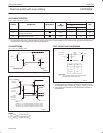
TEST CIRCUIT AND WAVEFORMS
C
L
= 50 pF
500 Ω
Load Circuit
DEFINITIONS
C
L
= Load capacitance includes jig and probe capacitance;
see AC CHARACTERISTICS for value.
TEST S1
t
pd
open
t
PLZ
/t
PZL
7 V
t
PHZ
/t
PZH
open
SA00012
500 Ω
From Output
Under Test
S1
7 V
Open
GND
NOTES:
1. All input pulses are supplied by generators having the following
characteristics: PRR ≤ 10 MHz, Z
O
= 50 Ω, t
r
≤ 2.5 ns, t
f
≤ 2.5 ns.
2. The outputs are measured one at a time with one transition per
measurement.