


Philips Semiconductors Product data
CBTD3306Dual bus switch with level shifting
2001 Nov 08
3
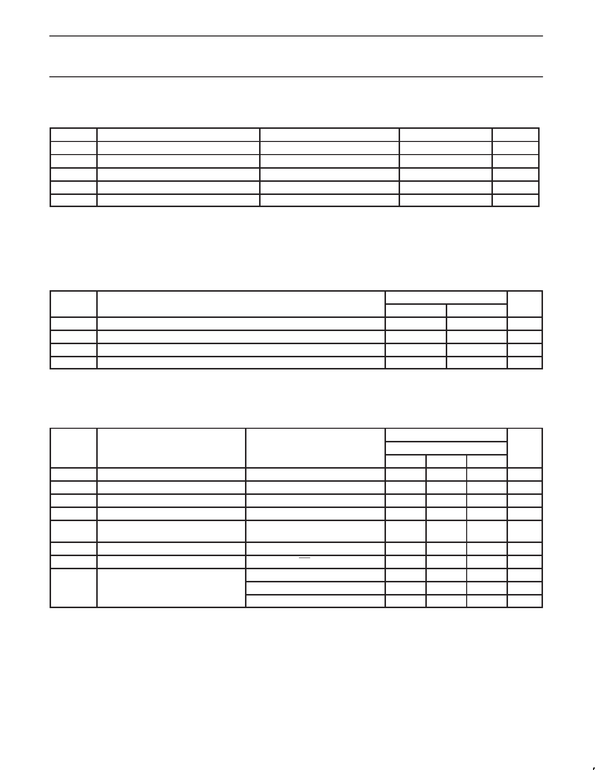
ABSOLUTE MAXIMUM RATINGS
1
T
amb
= –40 to +85 °C, unless otherwise specified.
SYMBOL
PARAMETER CONDITIONS RATING UNIT
V
CC
DC supply voltage –0.5 to +7.0 V
V
I
DC input voltage
2
–0.5 to +7.0 V
I
OUT
DC output current 128 mA
I
IK
Input diode current V
I/O
< 0 –50 mA
T
stg
Storage temperature range –65 to +150 °C
NOTES:
1. Stresses beyond those listed may cause permanent damage to the device. These are stress ratings only and functional operation of the
device at these or any other conditions beyond those indicated under “recommended operating conditions” is not implied. Exposure to
absolute-maximum-rated conditions for extended periods may affect device reliability.
2. The input and output negative-voltage ratings may be exceeded if the input and output clamp-current ratings are observed.
3. The package thermal impedance is calculated in accordance with JESD 51.
RECOMMENDED OPERATING CONDITIONS
1
SYMBOL
PARAMETER
LIMITS
UNIT
SYMBOL
PARAMETER
MIN MAX
UNIT
V
CC
DC supply voltage 4.5 5.5 V
V
IH
High-level input voltage 2.0 — V
V
IL
Low-level Input voltage — 0.8 V
T
amb
Operating free-air temperature range –40 +85 °C
NOTE:
1. All unused control inputs of the device must be held at V
CC
or GND to ensure proper device operation.
DC ELECTRICAL CHARACTERISTICS
T
amb
= –40 to +85 °C, unless otherwise specified.
LIMITS
SYMBOL PARAMETER TEST CONDITIONS T
amb
= –40 to +85 °C UNIT
MIN TYP
1
MAX
V
IK
Input clamp voltage V
CC
= 4.5 V; I
I
= –18 mA — — –1.2 V
I
I
Input leakage current V
CC
= 5.5 V; V
I
= GND or 5.5 V — — ±1 µA
I
CC
Quiescent supply current V
CC
= 5.5 V; I
O
= 0, V
I
= V
CC
or GND — — 1.5 mA
V
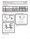
P
Output high pass voltage See Figure 1 — — — V
∆I
CC
Additional supply current per input pin
2
V
CC
= 5.5 V, one input at 3.4 V,
other inputs at V
CC
or GND
— — 2.5 mA
C
I
Control pins capacitance V
I
= 3 V or 0 — 3.20 — pF
C
IO(OFF)
Port off capacitance V
O
= 3 V or 0; OE = V
CC
— 6.50 — pF
3
V
CC
= 4.5 V; V
I
= 0V; I
I
= 64 mA — 3.6 5 Ω
r
on
3
On-resistance
V
CC
= 4.5 V; V
I
= 0 V; I
I
= 30 mA — 3.6 5 Ω
V
CC
= 4.5 V; V
I
= 2.4 V; I
I
= 15 mA — 17 35 Ω
NOTES:
1. All typical values are at V
CC
= 5 V, T
amb
= 25 °C.
2. This is the increase in supply current for each input that is at the specified TTL voltage level rather than V
CC
or GND
3. Measured by the voltage drop between the A and the B terminals at the indicated current through the switch.
On-state resistance is determined by the lowest voltage of the two (A or B) terminals.