


1999 May 31 4
Philips Semiconductors Product specification
Home automation modem TDA5051A
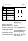
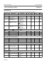
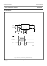
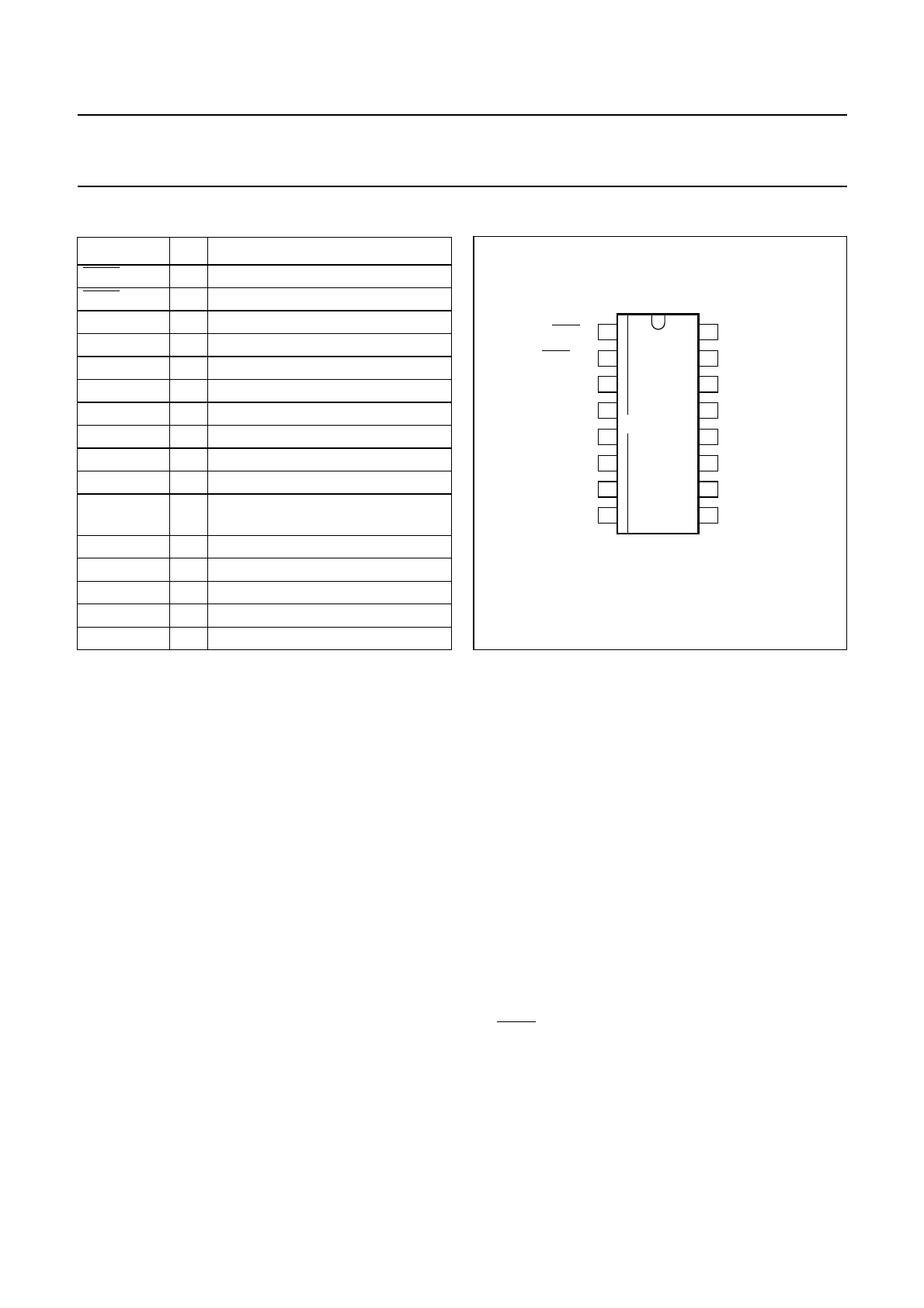
PINNING
SYMBOL PIN DESCRIPTION
DATA
IN
1 digital data input (active LOW)
DATA
OUT
2 digital data output (active LOW)
V
DDD
3 digital supply voltage
CLK
OUT
4 clock output
DGND 5 digital ground
SCANTEST 6 test input (LOW in application)
OSC1 7 oscillator input
OSC2 8 oscillator output
APGND 9 analog ground for power amplifier
TX
OUT
10 analog signal output
V
DDAP
11 analog supply voltage for power
amplifier
AGND 12 analog ground
V
DDA
13 analog supply voltage
RX
IN
14 analog signal input
PD 15 power-down input (active HIGH)
TEST1 16 test input (HIGH in application)
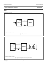
Fig.2 Pin configuration.
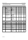
handbook, halfpage
TDA5051AT
MGK833
1
2
3
4
5
6
7
8
16
15
14
13
12
11
10
9
DATA
IN
DATA
OUT
V
DDD
CLK
OUT
DGND
SCANTEST
OSC1
OSC2
APGND
TX
OUT
V
DDAP
AGND
V
DDA
RX
IN
PD
TEST1
FUNCTIONAL DESCRIPTION
Both transmission and reception stages are controlled
either by the master clock of the microcontroller or by the
on-chip reference oscillator connected to a crystal. This
ensures the accuracy of the transmission carrier and the
exact trimming of the digital filter, thus making the
performance totally independent of application
disturbances such as component spread, temperature,
supply drift and so on.
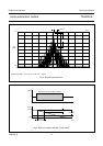
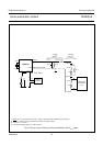
The interface with the power network is made by means of
an LC network (see Fig.18). The device includes a power
output stage that feeds a 120 dBµV (RMS) signal on a
typical 30 Ω load.
To reduce power consumption, the IC is disabled by a
power-down input (pin PD): in this mode, the on-chip
oscillator remains active and the clock continues to be
supplied at pin CLK
OUT
. For low-power operation in
reception mode, this pin can be dynamically controlled by
the microcontroller, see Section “Power-down mode”.
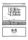
When the circuit is connected to an external clock
generator (see Fig.6), the clock signal must be applied at
pin OSC1 (pin 7); OSC2 (pin 8) must be left open-circuit.
Fig.7 shows the use of the on-chip clock circuit.
All logic inputs and outputs are compatible with
TTL/CMOS levels, providing an easy connection to a
standard microcontroller I/O port.
The digital part of the IC is fully scan-testable. Two digital
inputs, SCANTEST and TEST1, are used for production
test: these pins must be left open-circuit in functional mode
(correct levels are internally defined by pull-up or
pull-down resistors).
Transmission mode
To provide strict stability with respect to environmental
conditions, the carrier frequency is generated by scanning
the ROM memory under the control of the microcontroller
clock or the reference frequency provided by the on-chip
oscillator. High frequency clocking rejects the aliasing
components to such an extent that they are filtered by the
coupling LC network and do not cause any significant
disturbance. The data modulation is applied through
pin DATA
IN
and smoothly applied by specific digital circuits
to the carrier (shaping). Harmonic components are limited
in this process, thus avoiding unacceptable disturbance of
the transmission channel (according to CISPR16 and
EN50065-1 recommendations). A −55 dB Total Harmonic
Distortion (TDH) is reached when the typical LC coupling
network (or an equivalent filter) is used.