


1999 May 31 6
Philips Semiconductors Product specification
Home automation modem TDA5051A
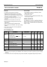
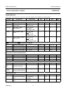
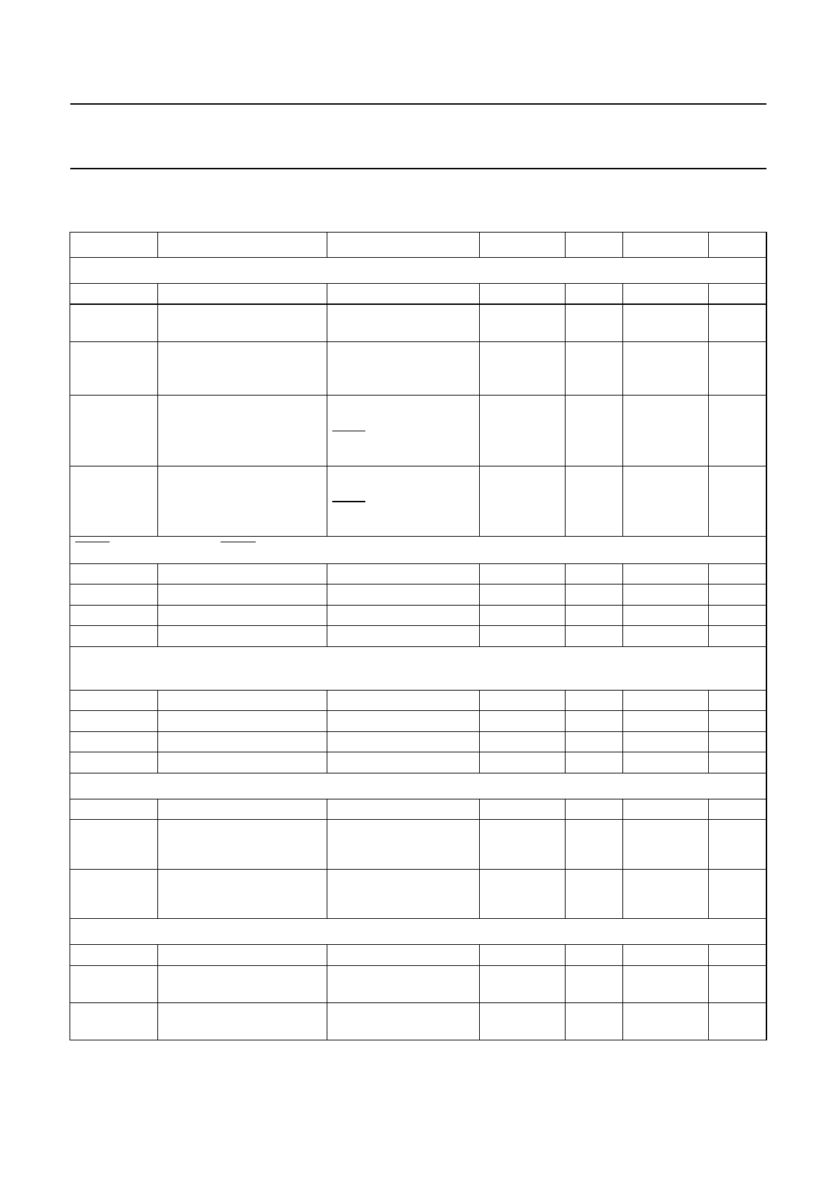
CHARACTERISTICS
V
DDD
=V
DDA
=5V±5%; T
amb
= 0 to 70 °C; V
DDD
connected to V
DDA
; DGND connected to AGND.
SYMBOL PARAMETER CONDITIONS MIN. TYP. MAX. UNIT
Supply
V
DD
supply voltage 4.75 5 5.25 V
I
DD(RX/TX)(tot)
total analog + digital
supply current
V
DD
=5V±5%
TX or RX mode
− 28 38 mA
I
DD(PD)(tot)
total analog + digital
supply current;
V
DD
=5V±5%;
PD = HIGH
Power-down mode
− 19 25 mA
I
DD(PAMP)
power amplifier supply
current
V
DD
=5V±5%;
Z
L
=30Ω;
DATA
IN
= LOW
in transmission mode
− 19 30 mA
I
DD(PAMP)(max)
maximum power amplifier
supply current
V
DD
=5V±5%;
Z
L
=1Ω;
DATA
IN
= LOW
in transmission mode
− 76 − mA
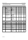
DATA
IN
and PD inputs: DATA
OUT
and CLK
OUT
outputs
V
IH
HIGH-level input voltage 0.2V
DD
+ 0.9 − V
DD
+ 0.5 V
V
IL
LOW-level input voltage −0.5 − 0.2V
DD
− 0.1 V
V
OH
HIGH-level output voltage I
OH
= −1.6 mA 2.4 −− V
V
OL
LOW-level output voltage I
OL
= 1.6 mA −−0.45 V
OSC1 input and OSC2 output (OSC2 only used for driving external quartz crystal; must be left open-circuit
when using an external clock generator)
V
IH
HIGH-level input voltage 0.7V
DD
− V
DD
+ 0.5 V
V
IL
LOW-level input voltage −0.5 − 0.2V
DD
− 0.1 V
V
OH
HIGH-level output voltage I
OH
= −1.6 mA 2.4 −− V
V
OL
LOW-level output voltage I
OL
= 1.6 mA −−0.45 V
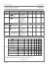
Clock
f
osc
oscillator frequency 6.080 − 9.504 MHz
ratio between oscillator
and carrier frequency
− 64 −
ratio between oscillator
and clock output frequency
− 2 −
Transmission mode
f
cr
carrier frequency f
osc
= 8.48 MHz − 132.5 − kHz
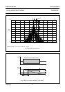
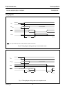
t
su
set-up time of the shaped
burst
f
osc
= 8.48 MHz;
see Fig.8
− 170 −µs
t
h
hold time of the shaped
burst
f
osc
= 8.48 MHz;
see Fig.8
− 170 −µs
f
osc
f
cr
--------
f
osc
f
CLKOUT
---------------------