


1999 Feb 16 6
Philips Semiconductors Preliminary specification
12-bit high-speed Analog-to-Digital
Converter (ADC)
TDA8767
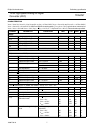
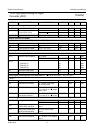
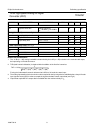
LIMITING VALUES
In accordance with the Absolute Maximum Rating System (IEC 134).
Note
1. The supply voltages V
CCA
, V
CCD
and V
CCO
may have any value between −0.3 V and +7.0 V provided that the supply
voltage differences ∆V
CC
are respected.
HANDLING
Inputs and outputs are protected against electrostatic discharges in normal handling. However, to be totally safe, it is
desirable to take normal precautions appropriate to handling integrated circuits.
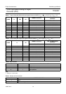
THERMAL CHARACTERISTICS
SYMBOL PARAMETER CONDITIONS MIN. MAX. UNIT
V
CCA
analog supply voltage note 1 −0.3 +7.0 V
V
CCD
digital supply voltage note 1 −0.3 +7.0 V
V
CCO
output supply voltage note 1 −0.3 +7.0 V
∆V
CC
supply voltage difference
V
CCA
− V
CCD
−1.0 +1.0 V
V
CCO
− V
CCD
−1.0 +4.0 V
V
CCA
− V
CCO
−1.0 +4.0 V
V
I
input voltage referenced to AGND 0.3 V
CCA
V
V
i(p-p)
input voltage for differential clock
drive (peak-to-peak value)
− V
CCD
V
I
O
output current − 10 mA
T
stg
storage temperature −55 +150 °C
T
amb
operating ambient temperature 0 70 °C
T
j
junction temperature − +150 °C
SYMBOL PARAMETER VALUE (TYP.) UNIT
R
th j-a
thermal resistance from junction to ambient in free air 75 K/W