


1999 Feb 16 8
Philips Semiconductors Preliminary specification
12-bit high-speed Analog-to-Digital
Converter (ADC)
TDA8767
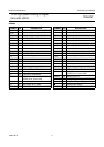
Voltage controlled regulator input V
ref
(referenced to V
CCA
)
V
ref(FS)
full scale fixed voltage V
CCA
=5V − 3.175 − V
V
i(p-p)
− V
i(p-p)
input voltage amplitude
(peak-to-peak value)
differential mode − 2.0 − V
single mode;
V
i
= 2.5 V − 2.0 − V
I
ref
input current at V
ref
− 10 −µA
Outputs (referenced to DGND)
D
IGITAL OUTPUTS D11 TO D0 AND IR (REFERENCED TO DGND)
V
OL
LOW-level output voltage I
OL
= 2 mA 0 − 0.5 V
V
OH
HIGH-level output voltage I
OH
= −0.4 mA V
CCO
− 0.5 − V
CCD
V
I
O
output current in 3-state 0.5 V < V
O
<V
CCO
−20 − +20 µA
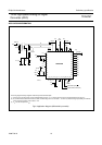
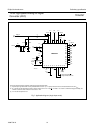
Switching characteristics
C
LOCK FREQUENCY f
clk
(see Fig.3)
f
clk(min)
minimum clock frequency SH = HIGH −−1 MHz
SH = LOW −−1 kHz
f
clk(max)
maximum clock frequency
TDA8767H/1 10 −−MHz
TDA8767H/2 20 −−MHz
TDA8767H/3 30 −−MHz
t
CPH
clock pulse width HIGH 8.5 −−ns
t
CPL
clock pulse width LOW 8.5 −−ns
Analog signal processing; 50% clock duty factor; V
i
− V
i
= 2.0 V; V
ref
=V
CCA
− 2V;see Table 1
L
INEARITY
ILE integral non-linearity f
clk
= 4 MHz; ramp input −±3.0 ±4.0 LSB
DLE differential non-linearity f
clk
= 4 MHz; ramp input;
no missing codes
−±0.6 ±1 LSB
OFER offset error V
CCA
=V
CCD
=V
CCO
=5V;
T
amb
=25°C; V
i
= V
i
; output
code = 2047
tbf − tbf LSB
GER gain error amplitude; spread
from device to device
V
CCA
=V
CCD
=V
CCO
=5V;
T
amb
=25°C; V
i
− V
i
= 2.0 V
tbf − tbf LSB
BANDWIDTH (f
clk
= 30 MHz); note 1
B analog bandwidth −1dB − 9 − MHz
−3dB − 18 − MHz
t
STLH
analog input settling time
LOW-to-HIGH transition
full scale square wave;
note 3
− tbf − ns
t
STHL
analog input settling time
HICH-to-LOW transition
full scale square wave;
note 3
− tbf − ns
HARMONICS
THD total harmonic distortion f
clk
= 30 MHz; f
i
= 4.43 MHz;
note 2
−−64 − dB
SYMBOL PARAMETER CONDITIONS MIN. TYP. MAX. UNIT