


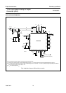
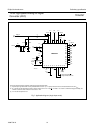
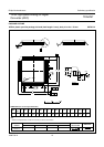

1999 Feb 16 7
Philips Semiconductors Preliminary specification
12-bit high-speed Analog-to-Digital
Converter (ADC)
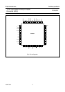
TDA8767
CHARACTERISTICS
V
CCA
=V
2
to V
44
, V
9
to V
10
, V
3
to V
4
and V
41
to V
40
= 4.75 to 5.25 V; V
CCD
=V
37
to V
38
and V
15
to V
17
= 4.75 to 5.25 V;
V
CCO
=V
33
to V
34
= 3.0 to 5.25 V; AGND and DGND shorted together; T
amb
= 0 to +70 °C; typical values measured at
V
CCA
=V
CCD
= 5 V and V
CCO
= 3.3 V; V
i(p-p)
− V
i(p-p)
= 2.0 V; C
L
= 15 pF and T
amb
=25°C; unless otherwise specified.
SYMBOL PARAMETER CONDITIONS MIN. TYP. MAX. UNIT
Supply
V
CCA
analog supply voltage 4.75 5.0 5.25 V
V
CCD
digital supply voltage 4.75 5.0 5.25 V
V
CCO
output supply voltage 3.0 3.3 5.25 V
I
CCA
analog supply current − 40 tbf mA
I
CCD
digital supply current − 22 tbf mA
I
CCO
output supply current f
clk
= 20 MHz; f
i
= 4.43 MHz − 12 tbf mA
Inputs
CLK (
REFERENCED TO DGND)
V
IL
LOW-level input voltage 0 − 0.8 V
V
IH
HIGH-level input voltage 2.0 − V
CCD
V
I
IL
LOW-level input current V
clk
= 0.3V
CCD
−400 −−µA
I
IH
HIGH-level input current V
clk
= 0.7V
CCD
−−100 µA
V
clk
=V
CCD
−−300 µA
Z
i
input impedance f
clk
= 30 MHz − 2 − kΩ
C
i
input capacitance f
clk
= 30 MHz − 2 − pF
TC; SH AND OE (REFERENCED TO DGND); see Tables 3 and 4
V
IL
LOW-level input voltage 0 − 0.8 V
V
IH
HIGH-level input voltage 2.0 − V
CCD
V
I
IL
LOW-level input current V
IL
= 0.3V
CCD
−400 −−µA
I
IH
HIGH-level input current V
IH
= 0.7V
CCD
−−20 µA
V
I
AND V
I
(REFERENCED TO AGND; see Tables 1 AND 2); V
ref
=V
CCA
− 2V
I
IL
LOW-level input current V
i
= V
i
− 10 −µA
I
IH
HIGH-level input current V
i
= V
i
− 10 −µA
Z
i
input impedance f
i
= 4.43 MHz − 10 − kΩ
C
i
input capacitance f
i
= 4.43 MHz − 2 − pF
V
ios(d)
input offset voltage in
differential mode
V
I
= V
I
; output code 2047
V
CCA
= 5 V tbf 2.5 tbf V
V
CCA
= 4.75 V tbf 2.25 tbf V
V
CCA
= 5.25 V tbf 2.75 tbf V
V
ios(s)
input offset voltage in single
mode
V
I
=V
ios(s)
; output
code 2047
V
CCA
= 5 V tbf 2.5 tbf V
V
CCA
= 4.75 V tbf 2.25 tbf V
V
CCA
= 5.25 V tbf 2.75 tbf V