


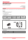
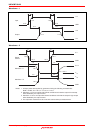
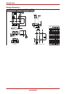
HD74CBT1G125
Rev.1.00 Apr 07, 2006 page 3 of 6
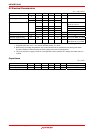
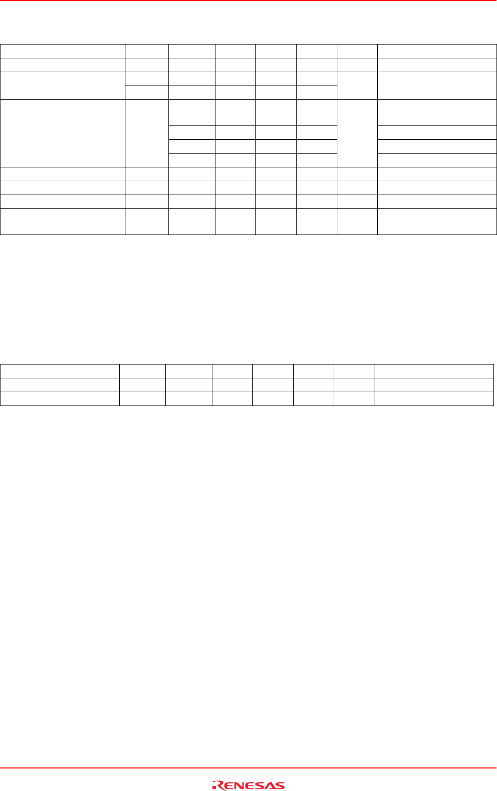
DC Electrical Characteristics
(Ta = −40 to 85°C)
Item Symbol V
CC
(V) Min Typ
*1
Max Unit Test conditions
Clamp diode voltage V
IK
4.5 −1.2 V I
IN
= −18 mA
V
IH
4.0 to 5.5 2.0 Input voltage
V
IL
4.0 to 5.5 0.8
V
4.0 14 20
V
IN
= 2.4 V, I
IN
= 15 mA
Typ at V
CC
= 4.0 V
4.5 5 7 V
IN
= 0 V, I
IN
= 64 mA
4.5 5 7 V
IN
= 0 V, I
IN
= 30 mA
On-state switch resistance
*2
R
ON
4.5 10 15
Ω
V
IN
= 2.4 V, I
IN
= 15 mA
Input current I
IN
0 to 5.5 ±1.0 µA V
IN
= 5.5 V or GND
Off-state leakage current I
OZ
5.5 ±1.0 µA 0 ≤ A, B ≤ V
CC
Quiescent supply current I
CC
5.5 1.0 µA V
IN
= V
CC
or GND, I
O
= 0 mA
Increase in I
CC
per input
*3
∆I
CC
5.5 2.5 mA
One input at 3.4 V,
other inputs at V
CC
or GND
Notes: For condition shown as Min or Max use the appropriate values under recommended operating conditions.
1. All typical values are at V
CC
= 5 V (unless otherwise noted), Ta = 25°C.
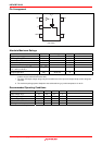
2. Measured by the voltage drop between the A and B terminals at the indicated current through the switch.
On-state resistance is determined by the lower voltage of the two (A or B) terminals.
3. This is the increase in supply current for each input that is at the specified TTL voltage level rather than V
CC
or GND.
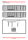
Capacitance
(Ta = 25°C)
Item Symbol V
CC
(V) Min Typ Max Unit Test conditions
Control input capacitance C
IN
5.0 3 pF V
IN
= 0 or 3 V
Input / output capacitance C
I/O (OFF)
5.0 5 pF V
O
= 0 or 3 V, OE = V
CC
Note: This parameter is determined by device characterization is not production tested.