


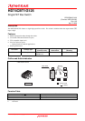
HD74CBT1G125
Rev.1.00 Apr 07, 2006 page 4 of 6
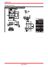
Switching Characteristics
(Ta = −40 to 85°C)
V
CC
= 4.0 V
Item Symbol Min Max Unit Test conditions
FROM
(Input)
TO
(Output)
Propagation delay time
*1
t
PLH
t
PHL
0.35 ns
C
L
= 50 pF
R
L
= 500 Ω
A or B B or A
Enable time
t
ZH
t
ZL
5.5 ns
C
L
= 50 pF
R
L
= 500 Ω
OE A or B
t
HZ
4.5 Disable time
t
LZ
4.5
ns
C
L
= 50 pF
R
L
= 500 Ω
OE A or B
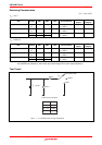
V
CC
= 5.0±0.5 V
Item Symbol Min Max Unit Test conditions
FROM
(Input)
TO
(Output)
Propagation delay time
*1
t
PLH
t
PHL
0.25 ns
C
L
= 50 pF
R
L
= 500 Ω
A or B B or A
Enable time
t
ZH
t
ZL
1.6 4.9 ns
C
L
= 50 pF
R
L
= 500 Ω
OE A or B
t
HZ
1.0 4.2 Disable time
t
LZ
1.0 4.8
ns
C
L
= 50 pF
R
L
= 500 Ω
OE A or B
Note: 1. The propagation delay is the calculated RC time constant of the typical on-state resistance of the switch and
the specified load capacitance, when driven by an ideal voltage source (zero output impedance).
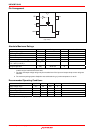
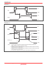
Test Circuit
OPEN
S1
C
L
= 50 pF
*1
500 Ω
Load circuit for outputs
Symbol
t / t
PLH PHL
t / t
ZH HZ
t / t
ZL LZ
S1
OPEN
OPEN
7 V
500 Ω
See under table
GND
Note: 1. C
L
includes probe and jig capacitance.