


HD74LVC1G66
Rev.3.00 Jul. 01, 2004 page 2 of 10
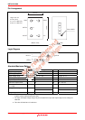
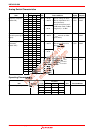
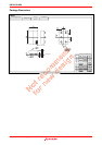
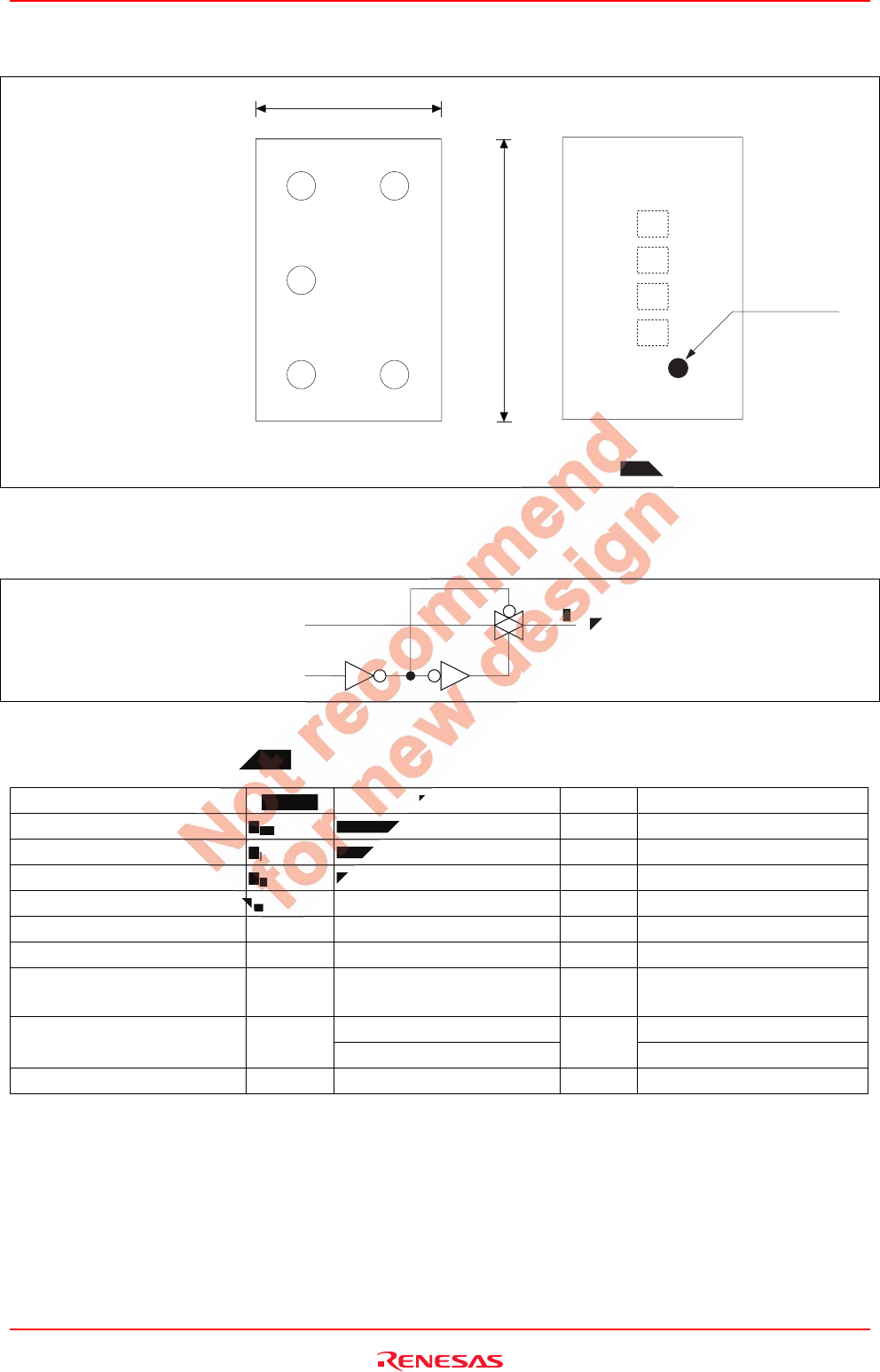
Pin Arrangement
(Bottom view) (Top view)
CONT
15
2
34GND
Height 0.5 mm
0.5 mm pitch
0.17 mm 5–Ball (CP)
0.23 mm 5–Ball (CL)
0.9 mm
1.4 mm
OUT/IN
IN/OUT
V
CC
Pin#1 INDEX
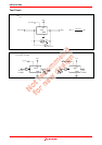
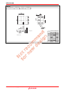
Logic Diagram
IN/OUT OUT/IN
CONT
1
4
2
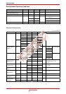
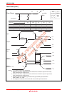
Absolute Maximum Ratings
Item Symbol Ratings Unit Test Conditions
Supply voltage range V
CC
–0.5 to 6.5 V
Input voltage range
*1
V
I
–0.5 to 6.5 V
Output voltage range
*1, 2
V
O
–0.5 to V
CC
+0.5 V Output : H or L
Control Input clamp current I
IK
–50 mA V
I
< 0
Output clamp current I
OK
±50 mA V
O
< 0 or V
O
> V
CC
Continuous output current I
O
±50 mA V
O
= 0 to V
CC
Continuous current through
V
CC
or GND
I
CC
or I
GND
±100 mA
154 CPPackage Thermal impedance θ
ja
132
°C/W
CL
Storage temperature Tstg –65 to 150 °C
Notes: The absolute maximum ratings are values, which must not individually be exceeded, and furthermore no two
of which may be realized at the same time.
1. The input and output voltage ratings may be exceeded if the input and output clamp-current ratings are
observed.
2. This value is limited to 5.5 V maximum.
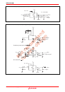
(Top view)
OUT/IN
2
Absolute Maximum Ratings
Symbol
Ratings
V
CC
–0.5 to 6.5
V
I
–0.5 to 6.5
V
O
–0.5 to V
Control Input clamp current I
IK