


HD74LVC1G66
Rev.3.00 Jul. 01, 2004 page 7 of 10
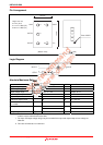
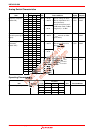
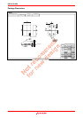
Test Circuit (cont.)
OPEN
OPEN
TEST S1
VTT
VTT
S1
C
L
R
L
R
L
GND
GND
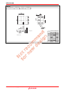
t / t
PLH PHL
t / t
ZH HZ
t / t
ZL LZ
1.8±0.15
2.5±0.2
3.3±0.3
5.0±0.5
INPUTS
V
CC
(V)
V
CC
2 × V
CC
2 × V
CC
2 × V
CC
2 × V
CC
V
CC
/ 2
V
CC
/ 2
V
CC
/ 2
V
CC
/ 2
V
CC
V
CC
V
CC
V
I
V
ref
C
L
R
L
∆VVTT
t
r
/ t
f
500 Ω
0.15 V
0.15 V
0.3 V
0.3 V
500 Ω
500 Ω
1.0 kΩ
Load circuit
From Output
≤ 2 ns
≤ 2 ns
≤ 2.5 ns
≤ 2.5 ns
30 pF
30 pF
50 pF
50 pF
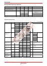
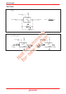
V
ref
V
ref
V
ref
V
ref
V
I
0 V
t
PLH
V
t
PHL
OH
V
OL
Input
Output
V
OH
V
OL
Control
Input
V
ref
V
ref
V
ref
V
OH
– ∆V
V
OL
+ ∆V
V
ref
V
I
V
OH
0 V
V
OL
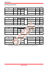
t
HZ
t
LZ
t
ZH
t
ZL
Output
(Waveform – A)
Output
(Waveform – B)
Notes: 1. C
L
includes probe and jig capacitance.
2. Waveform–A is for an output with internal conditions such that the output is low except
when disabled by the output control.
3. Waveform–B is for an output with internal conditions such that the output is high except
when disabled by the output control.
4. All input pulses are supplied by generators having the following characteristics:
PRR ≤ 10MHz, Zo = 50 Ω.
5. The output are measured one at a time with one transition per measurement.
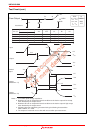
V
ref
t
PHL
V
ref
t
ZL
V
ref
t
ZH