


- 3 -
datasheet DDR3L SDRAM
Rev. 1.0
Unbuffered DIMM
Table Of Contents
240pin Unbuffered DIMM based on 2Gb D-die
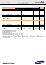
1. DDR3L Unbuffered DIMM Ordering Information...........................................................................................................4
2. Key Features.................................................................................................................................................................4
3. Address Configuration ..................................................................................................................................................4
4. x72 DIMM Pin Configurations (Front side/Back side) ...................................................................................................5
5. Pin Description .............................................................................................................................................................6
6. SPD and Thermal Sensor for ECC UDIMMs ................................................................................................................6
7. Input/Output Functional Description..............................................................................................................................7
7.1 Address Mirroring Feature....................................................................................................................................... 8
7.1.1. DRAM Pin Wiring Mirroring.............................................................................................................................. 8
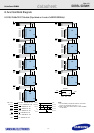
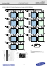
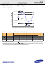
8. Function Block Diagram:...............................................................................................................................................9
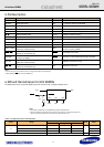
8.1 2GB, 256Mx72 ECC Module (Populated as 1 rank of x8 DDR3 SDRAMs) ............................................................ 9
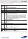
8.2 4GB, 512Mx72 ECC Module (Populated as 2 ranks of x8 DDR3 SDRAMs)...........................................................10
9. Absolute Maximum Ratings..........................................................................................................................................11
9.1 Absolute Maximum DC Ratings...............................................................................................................................11
9.2 DRAM Component Operating Temperature Range ................................................................................................11
10. AC & DC Operating Conditions...................................................................................................................................11
10.1 Recommended DC Operating Conditions (SSTL-15)............................................................................................11
11. AC & DC Input Measurement Levels..........................................................................................................................12
11.1 AC & DC Logic Input Levels for Single-ended Signals..........................................................................................12
11.2 V
REF
Tolerances....................................................................................................................................................14
11.3 AC and DC Logic Input Levels for Differential Signals ..........................................................................................15
11.3.1. Differential Signals Definition.........................................................................................................................15
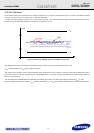
11.3.2. Differential Swing Requirement for Clock (CK - CK
) and Strobe (DQS - DQS).............................................15
11.3.3. Single-ended Requirements for Differential Signals ......................................................................................17
11.3.4. Differential Input Cross Point Voltage ............................................................................................................18
11.4 Slew Rate Definition for Single Ended Input Signals.............................................................................................19
11.5 Slew rate definition for Differential Input Signals...................................................................................................19
12. AC & DC Output Measurement Levels.......................................................................................................................19
12.1 Single Ended AC and DC Output Levels...............................................................................................................19
12.2 Differential AC and DC Output Levels...................................................................................................................19
12.3 Single-ended Output Slew Rate ............................................................................................................................20
12.4 Differential Output Slew Rate ................................................................................................................................21
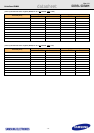
13. IDD specification definition..........................................................................................................................................22
14. IDD SPEC Table.........................................................................................................................................................24
15. Input/Output Capacitance...........................................................................................................................................25
16. Electrical Characteristics and AC timing.....................................................................................................................26
16.1 Refresh Parameters by Device Density.................................................................................................................26
16.2 Speed Bins and CL, tRCD, tRP, tRC and tRAS for Corresponding Bin ................................................................26
16.3 Speed Bins and CL, tRCD, tRP, tRC and tRAS for corresponding Bin.................................................................26
16.3.1. Speed Bin Table Notes..................................................................................................................................28
17. Timing Parameters by Speed Grade ..........................................................................................................................30
17.1 Jitter Notes ............................................................................................................................................................33
17.2 Timing Parameter Notes........................................................................................................................................34
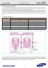
18. Physical Dimensions...................................................................................................................................................35
18.1 256Mbx8 based 256Mx72 Module (1 Rank) - M391B5773DH0............................................................................35
18.2 256Mbx8 based 512Mx72 Module (2 Ranks) - M391B5273DH0..........................................................................36