


- 31 -
datasheet DDR3L SDRAM
Rev. 1.0
Unbuffered DIMM
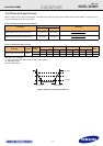
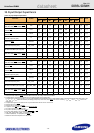
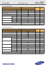
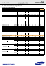
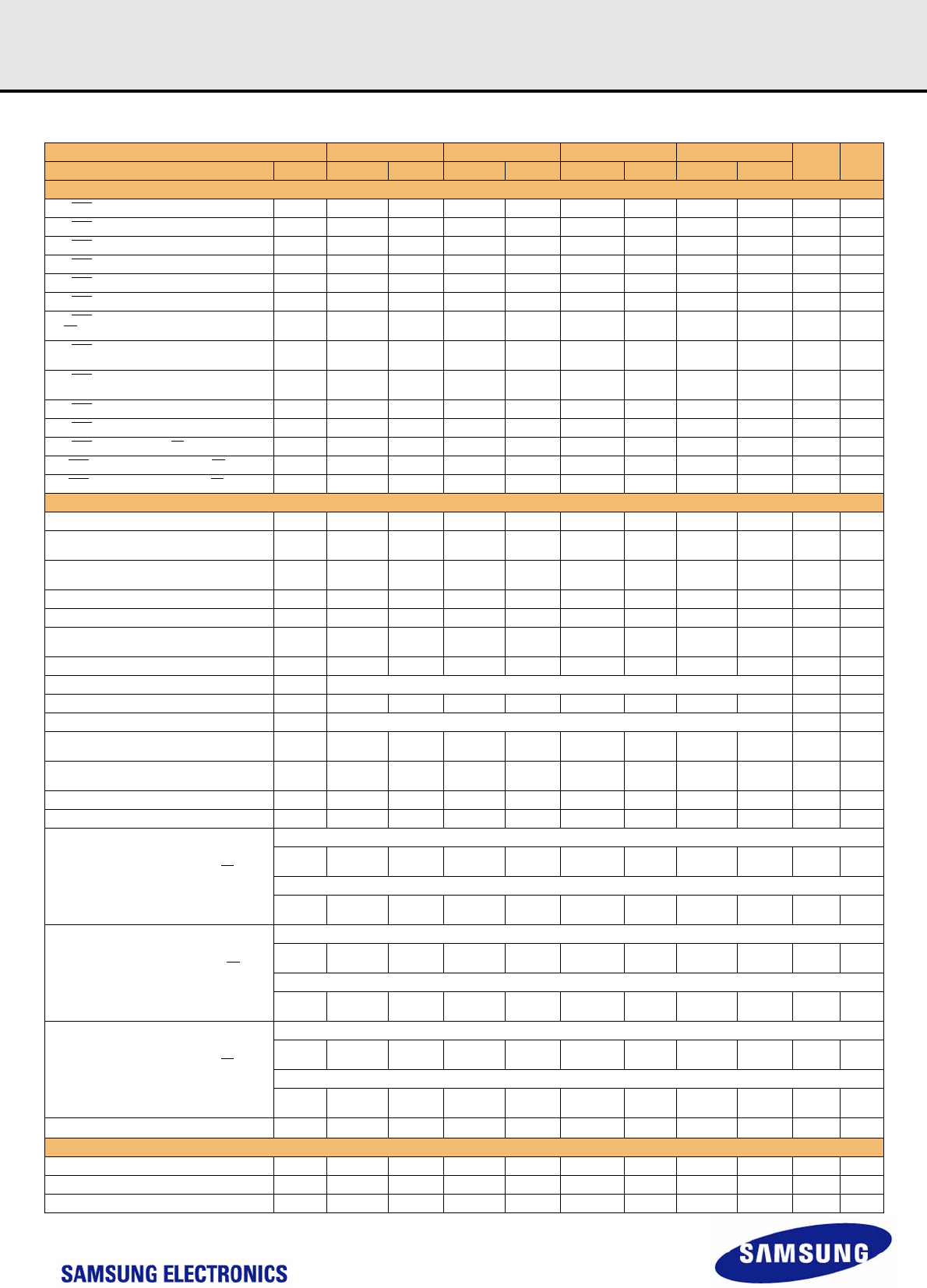
[ Table 21 ] Timing Parameters by Speed Bin (Cont.)
Speed DDR3-800 DDR3-1066 DDR3-1333 DDR3-1600
Units NOTE
Parameter Symbol MIN MAX MIN MAX MIN MAX MIN MAX
Data Strobe Timing
DQS, DQS differential READ Preamble tRPRE 0.9 Note 19 0.9 Note 19 0.9 Note 19 0.9 Note 19 tCK 13, 19, g
DQS, DQS differential READ Postamble tRPST 0.3 Note 11 0.3 Note 11 0.3 Note 11 0.3 Note 11 tCK 11, 13, b
DQS, DQS differential output high time tQSH 0.38 - 0.38 - 0.4 - 0.4 - tCK(avg) 13, g
DQS, DQS differential output low time tQSL 0.38 - 0.38 - 0.4 - 0.4 - tCK(avg) 13, g
DQS, DQS differential WRITE Preamble tWPRE 0.9 - 0.9 - 0.9 - 0.9 - tCK
DQS, DQS differential WRITE Postamble tWPST 0.3 - 0.3 - 0.3 - 0.3 - tCK
DQS, DQS rising edge output access time from rising
CK, CK
tDQSCK -400 400 -300 300 -255 255 -225 225 ps 13,f
DQS, DQS low-impedance time (Referenced from RL-
1)
tLZ(DQS) -800 400 -600 300 -500 250 -450 225 ps 13,14,f
DQS, DQS high-impedance time (Referenced from
RL+BL/2)
tHZ(DQS) - 400 - 300 - 250 - 225 ps 12,13,14
DQS, DQS differential input low pulse width tDQSL 0.45 0.55 0.45 0.55 0.45 0.55 0.45 0.55 tCK 29, 31
DQS, DQS differential input high pulse width tDQSH 0.45 0.55 0.45 0.55 0.45 0.55 0.45 0.55 tCK 30, 31
DQS, DQS rising edge to CK, CK rising edge tDQSS -0.25 0.25 -0.25 0.25 -0.25 0.25 -0.27 0.27 tCK(avg) c
DQS,DQS falling edge setup time to CK, CK rising edge tDSS 0.2 - 0.2 - 0.2 - 0.18 - tCK(avg) c, 32
DQS,DQS falling edge hold time to CK, CK rising edge tDSH 0.2 - 0.2 - 0.2 - 0.18 - tCK(avg) c, 32
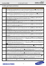
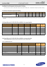
Command and Address Timing
DLL locking time tDLLK 512 - 512 - 512 - 512 - nCK
internal READ Command to PRECHARGE Command
delay
tRTP
max
(4nCK,7.5ns)
-
max
(4nCK,7.5ns)
-
max
(4nCK,7.5ns)
-
max
(4nCK,7.5ns)
- e
Delay from start of internal write transaction to internal
read command
tWTR
max
(4nCK,7.5ns)
-
max
(4nCK,7.5ns)
-
max
(4nCK,7.5ns)
-
max
(4nCK,7.5ns)
- e,18
WRITE recovery time tWR 15 - 15 - 15 - 15 - ns e
Mode Register Set command cycle time tMRD 4 - 4 - 4 - 4 - nCK
Mode Register Set command update delay tMOD
max
(12nCK,15ns)
-
max
(12nCK,15ns)
-
max
(12nCK,15ns)
-
max
(12nCK,15ns)
-
CAS# to CAS# command delay tCCD 4 - 4 - 4 - 4 - nCK
Auto precharge write recovery + precharge time tDAL(min) WR + roundup (tRP / tCK(AVG)) nCK
Multi-Purpose Register Recovery Time tMPRR 1 - 1 - 1 - 1 - nCK 22
ACTIVE to PRECHARGE command period tRAS See “Speed Bins and CL, tRCD, tRP, tRC and tRAS for corresponding Bin” ns e
ACTIVE to ACTIVE command period for 1KB page size tRRD
max
(4nCK,10ns)
-
max
(4nCK,7.5ns)
-
max
(4nCK,6ns)
-
max
(4nCK,6ns)
- e
ACTIVE to ACTIVE command period for 2KB page size tRRD
max
(4nCK,10ns)
-
max
(4nCK,10ns)
-
max
(4nCK,7.5ns)
-
max
(4nCK,7.5ns)
- e
Four activate window for 1KB page size tFAW 40 - 37.5 - 30 - 30 - ns e
Four activate window for 2KB page size tFAW 50 - 50 - 45 - 40 - ns e
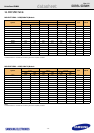
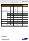
Command and Address setup time to CK, CK refer-
enced to V
IH
(AC) / V
IL
(AC) levels
1.35V
tIS(base)
AC160
215
-
140
-
80 - 60 - ps b,16
1.5V
tIS(base)
AC175
200
-
125
-
65 - 45 - ps b,16
Command and Address hold time from CK, CK refer-
enced to V
IH
(AC) / V
IL
(AC) levels
1.35V
tIH(base)
DC90
285
-
210
-
150 - 130 - ps b,16
1.5V
tIH(base)
DC100
275 200 140 120 - ps b,16
Command and Address setup time to CK, CK refer-
enced to V
IH
(AC) / V
IL
(AC) levels
1.35V
tIS(base)
AC135
365
-
290
-
205 - 185 - ps b,16,27
1.5V
tIS(base)
AC150
350
-
275
-
190 - 170 - ps b,16,27
Control & Address Input pulse width for each input tIPW 900
-
780
-
620 - 560 - ps 28
Calibration Timing
Power-up and RESET calibration time tZQinitI 512 - 512 - 512 - 512 - nCK
Normal operation Full calibration time tZQoper 256 - 256 - 256 - 256 - nCK
Normal operation short calibration time tZQCS 64 - 64 - 64 - 64 - nCK 23