


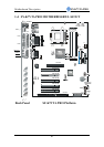
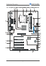

Motherboard Description
SY-K7VTA PRO
12
1-8 CHIPSET
VT8363A
The KT133A chip set consists of the VT8363A system controller (552 pin
BGA) and the VT82C686B PCI to ISA bridge (352 pin BGA). The
system controller provides superior performance between the CPU,
DRAM, AGP bus, and PCI bus with pipelined, burst, and concurrent
operation.
The VT8363A support six banks of DRAMs up to 1.5GB. The DRAM
controller supports standard Synchronous DRAM (SDRAM) and Virtual
Channel SDRAM (VC SDRAM), in a flexible mix / match manner. The
Synchronous DRAM interface allows zero wait state bursting between the
DRAM and the data buffers at 66/100/133 MHz. The six banks of
DRAM can be composed of an arbitrary mixture of 1M / 2M / 4M / 8M /
16M / 32MxN DRAMs.
The VT8363A system controller also supports full AGP v2.0 capability for
maximum bus utilization including 1x, 2x and 4x mode transfers, SBA
(SideBand Addressing), Flush/fence commands, and pipelined grants.
An eight level request queue plus a four level post-write request queue
with thirty-two and sixteen quadwords of read and write data FIFO’s
respectively are included for deep pipelined and split AGP transactions.
A single-level GART TLB with 16 full associative entries and flexible
CPU / AGP / PCI remapping control is also provided for operation under
protected mode operating environments. Both Windows-95 VXD and
Windows-98 / Windows 2000 miniport drivers are supported for
interoperability with major AGP-based 3D and DVD-capable multimedia
accelerators.
The VT8363A supports two 32-bit 3.3 / 5V system buses (one AGP and
one PCI) that are synchronous / pseudo-synchronous to the CPU bus.
The chip also contains a built-in bus-to-bus bridge to allow simultaneous
concurrent operations on each bus. Five levels (doublewords) of post
write buffers are included to allow for concurrent CPU and PCI operation.
For PCI master operation, forty-eight levels (doublewords) of post write