


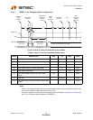
USB 2.0 Hi-Speed Hub Controller
Datasheet
Revision 1.0 (3-11-09) 60 SMSC USB251x
DATASHEET
Chapter 9 DC Parameters
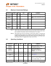
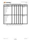
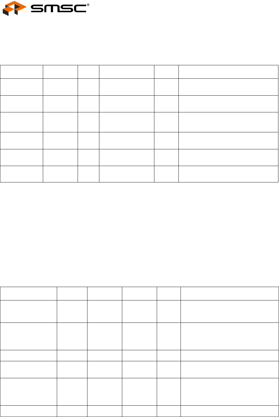
9.1 Maximum Guaranteed Ratings
Note 9.1 Stresses above the specified parameters could cause permanent damage to the device.
This is a stress rating only and functional operation of the device at any condition above
those indicated in the operation sections of this specification is not implied.
Note 9.2 When powering this device from laboratory or system power supplies, it is important that
the absolute maximum ratings not be exceeded or device failure can result. Some power
supplies exhibit voltage spikes on their outputs when the AC power is switched on or off.
In addition, voltage transients on the AC power line may appear on the DC output. When
this possibility exists, it is suggested that a clamp circuit be used.
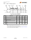
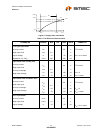
9.2 Operating Conditions
PARAMETER SYMBOL MIN MAX UNITS COMMENTS
Storage
Temperature
T
STOR
-55 150 °C
Lead
Temperature
Refer to JEDEC Specification J-STD-
020D.
3.3 V supply
voltage
VDD33
PLLFILT
CRFILT
4.6 V Applies to all parts.
Voltage on any
I/O pin
-0.5 5.5 V
Voltage on
XTALIN
-0.5 4.0 V
Voltage on
XTALOUT
-0.5 2.5 V
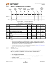
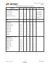
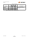
PARAMETER SYMBOL MIN MAX UNITS COMMENTS
Commercial
Operating
Temperature
T
A
0 70 °C Ambient temperature in still air.
Only applies to USB251x, USB251xA,
and USB251xB products.
Industrial
Operating
Temperature
T
AI
-40 85 °C Ambient temperature in still air.
Only applies to USB251xi,
USB251xAi, and USB251xBi
products.
3.3 V supply voltage
VDD33 3.0 3.6 V Applies to all parts.
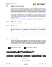
3.3 V supply rise
time
t
RT
0 400 μs See Figure 9.1
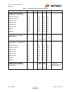
Voltage on any I/O
pin
-0.3 5.5 V If any 3.3 V supply voltage drops
below 3.0 V, then the MAX becomes:
(3.3 V supply voltage) + 0.5
Voltage on XTALIN -0.3
VDD33 V