


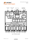
USB 2.0 High-Speed 4-Port Hub Controller
Datasheet
SMSC USB2514 13 Revision 1.98 (11-19-07)
DATASHEET
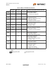
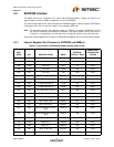
CFG_SEL2 n/a 33 I Configuration Programming Select
Note: This pin is not available in all packages; it is
held to a logic ‘0’ when not available
The logic state of this pin is internally latched on the
rising edge of RESET_N (RESET_N negation), and will
determine the hub configuration method as described in
Table 3.2, "SMBus or EEPROM Interface Behavior"
MISC
XTAL1/
CLKIN
33 45 ICLKx Crystal Input/External Clock Input
24MHz crystal or external clock input.
This pin connects to either one terminal of the crystal or
to an external 24/48MHz clock when a crystal is not
used.
Note: 48MHz only available in 48 QFN.
XTAL2 32 44 OCLKx Crystal Output
24MHz Crystal
This is the other terminal of the crystal, or pulled high
when an external clock source is used to drive
XTAL1/CLKIN. This output must not be used to drive
any external circuitry other than the crystal circuit.
RESET_N 26 34 IS RESET Input
The system can reset the chip by driving this input low.
The minimum active low pulse is 1 us.
When the RESET_N pin is pulled to VDD33, the internal
POR (Power on Reset) is enabled and no external reset
circuitry is required. The internal POR holds the internal
logic in reset until the power supplies are stable.
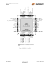
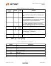
Table 3.1 USB2514 Pin Descriptions (continued)
SYMBOL 36 QFN 48 QFN
BUFFER
TYPE DESCRIPTION