


Small Footprint Hi-Speed USB 2.0 Device PHY with UTMI Interface
Datasheet
Revision 1.5 (11-02-07) 12 SMSC USB3290
DATASHEET
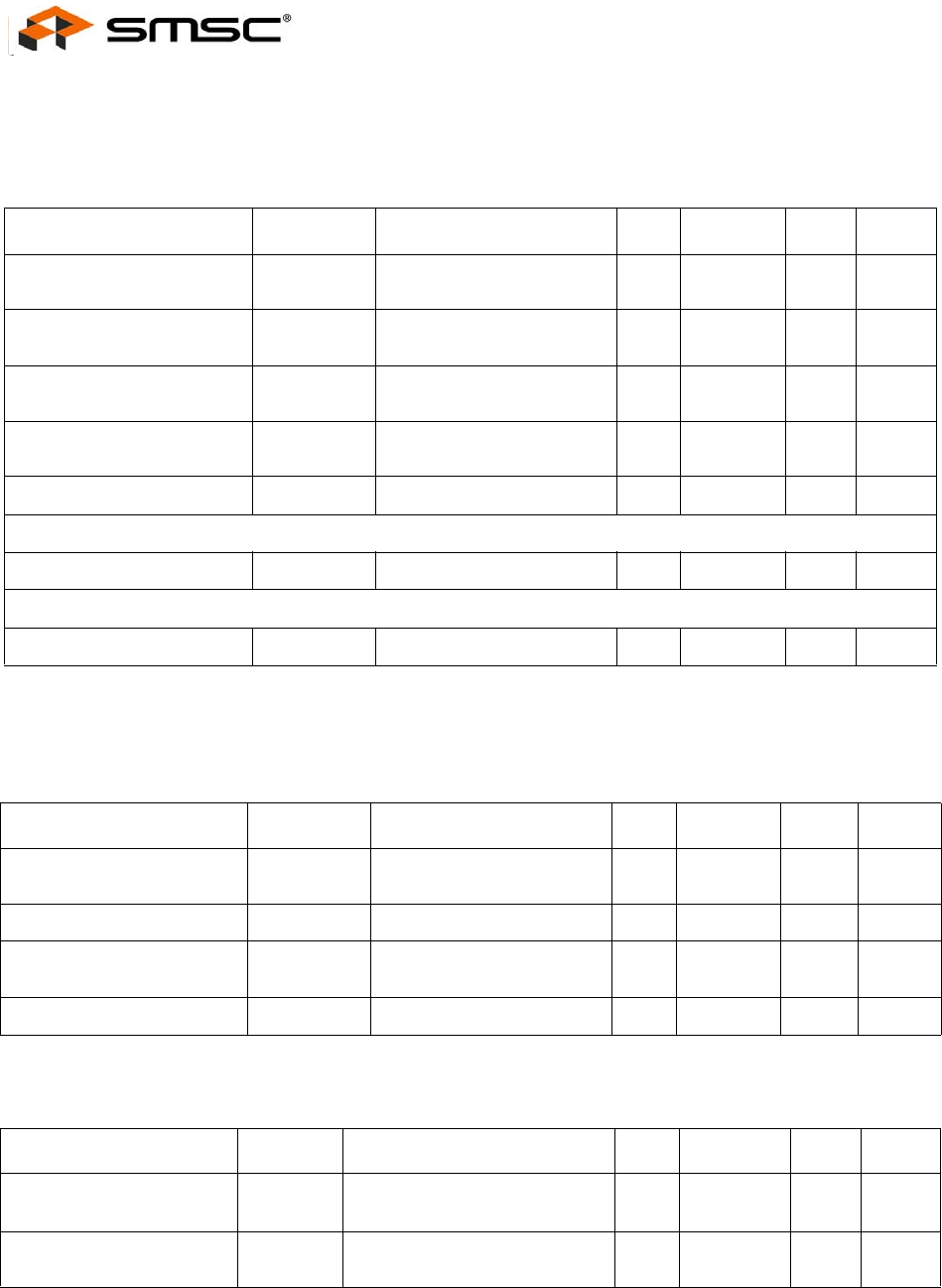
Chapter 5 Limiting Values
Note: In accordance with the Absolute Maximum Rating system (IEC 60134)
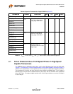
Table 5.1 Absolute Maximum Ratings
PARAMETER SYMBOL CONDITIONS MIN TYP MAX UNITS
Maximum DP and DM
voltage to Ground
V
MAX_5V
-0.3 5.5 V
Maximum VDD1.8 and
VDDA1.8 voltage to Ground
V
MAX_1.8V
-0.3 2.5 V
Maximum 3.3V Supply
Voltage to Ground
V
MAX_3.3V
-0.3 4.0 V
Maximum I/O Voltage to
Ground
V
I
-0.3 4.0 V
Storage Temperature T
STG
-55 150
o
C
ESD PERFORMANCE
All Pins V
HBM
Human Body Model ±5 kV
LATCH-UP PERFORMANCE
All Pins I
LTCH_UP
EIA/JESD 78, Class II 150 mA
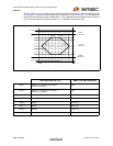
Table 5.2 Recommended Operating Conditions
PARAMETER SYMBOL CONDITIONS MIN TYP MAX UNITS
3.3V Supply Voltage
(VDD3.3 and VDDA3.3)
V
DD3.3
3.0 3.3 3.6 V
Input Voltage on Digital Pins V
I
0.0 V
DD3.3
V
Input Voltage on Analog I/O
Pins (DP, DM)
V
I(I/O)
0.0 V
DD3.3
V
Ambient Temperature T
A
-40 85
o
C
Table 5.3 Recommended External Clock Conditions
PARAMETER SYMBOL CONDITIONS MIN TYP MAX UNITS
System Clock Frequency XO driven by the external
clock; and no connection at XI
24
(±100ppm)
MHz
System Clock Duty Cycle XO driven by the external
clock; and no connection at XI
45 50 55 %