


USB 2.0 Flash Drive Controller
Datasheet
SMSC USB97C242 Page 11 Revision 1.4 (05-03-07)
DATASHEET
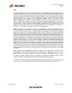
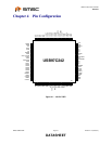
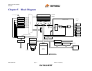
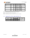
Chapter 5 Block Diagram
Flash
Media
DMA
Unit
D
a
t
a
B
u
s
s
USB 2.0 PHY
( Transciever )
FAST 8051
CPU CORE
GPIO 7 pins
7 pins
Configuration and Control
Clock Generation
XTAL
SIE
( Serial Interface Engine )
Program Memory/ IO
Bus
Interrupt Controller
Latch phase 0, 2
SIE
Latch phase 3
8051
Latch phase 1
FMC
60MHz32 Bit
Osc
Address
XDATA & SFR
Address and Data busses
64 Bytes EP0TX
64 Bytes EP0RX
64 Bytes EP1TX
64 Bytes EP1RX
Auto address generators
Address MUX
Data @ 32 bit
15Mhz
SIE Control Regs
Address
Address
Address
Address
EP0RX_BC
RAMRD_A/B
EP0TX_BC
RAMWR_A/B
32 bit 15MHz Data Buss
CLOCKOUT
12 MHz
512 Bytes EP2 TX/RX Buffer A
Address Register
1.25KB
SRAM
12K Byte
Scratchpad
SRAM
Clocked byPhase 0, 2 Clock
Clocked by Phase 3 Clock
512 Bytes EP2 TX/RX Buffer B
Memory
Cards
Scratchpad
SRAM (768 Byte)
ECC
Control/
Status
Flash Media
Controller (FMC)
SM
Controller
NAND Flash
Control/
Status
MEM/IO Bus 29pins
DATA
EP1TX_BC
EP1RX_BC
Address
Address
NAND Flash
SM/
NAND Flash
NAND Flash
CS[7:0]
48KB ROM
ROMEN
NAND Flash
NAND Flash
NAND Flash
NAND Flash