


USB 2.0 Flash Drive Controller
Datasheet
SMSC USB97C242 Page 16 Revision 1.4 (05-03-07)
DATASHEET
Chapter 7 DC Parameters
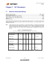
7.1 Maximum Guaranteed Ratings
Operating Temperature Range........................................................................................................................... 0
o
C to +70
o
C
Storage Temperature Range............................................................................................................................-55
o
to +150
o
C
Lead Temperature Range (soldering, 10 seconds)..................................................................................................... +325
o
C
Positive Voltage on any pin, with respect to Ground ........................................................................................................5.5V
Negative Voltage on any pin, with respect to Ground......................................................................................................-0.3V
Maximum V
DD,
V
DDP
........................................................................................................................................................+3.0V
Maximum V
DDIO,
V
DDA
......................................................................................................................................................+4.0V
*Stresses above the specified parameters could cause permanent damage to the device. This is a stress rating only and
functional operation of the device at any other condition above those indicated in the operation sections of this
specification is not implied.
Note: When powering this device from laboratory or system power supplies, it is important that the Absolute
Maximum Ratings not be exceeded or device failure can result. Some power supplies exhibit voltage
spikes on their outputs when the AC power is switched on or off. In addition, voltage transients on the AC
power line may appear on the DC output. When this possibility exists, it is suggested that a clamp circuit
be used.
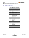
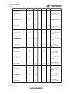
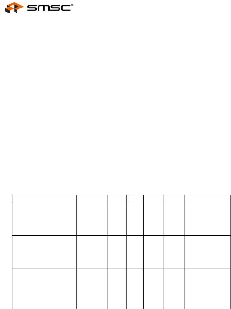
Table 7.1 - DC Electrical Characteristics
(T
A
= 0°C - 70°C, V
DDIO,
V
DDA
= +3.3 V ± 10%, V
DD,
V
DDP
= +2.5 V ± 10%,)
PARAMETER SYMBOL MIN TYP MAX UNITS COMMENTS
I Type Input Buffer
Low Input Level
High Input Level
V
ILI
V
IHI
2.0
0.8
V
V
TTL Levels
ICLK Input Buffer
Low Input Level
High Input Level
V
ILCK
V
IHCK
2.2
0.4
V
V
Input Leakage
(All I and IS buffers)
Low Input Leakage
High Input Leakage
I
IL
I
IH
-10
-10
+10
+10
uA
uA
V
IN
= 0
V
IN
= V
DDIO