ADS5102/3 EVM Operational Procedure
1-3
Overview
1.4 ADS5102/3 EVM Operational Procedure
The ADS5102/3 EVM provides a flexible means of evaluating the ADS5102/3
in a number of modes of operation. A basic setup procedure that can be used
as a board confidence check is as follows:
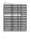
1) Verify all jumper settings against the schematic jumper list in Table 1–1
and Table 1–2:
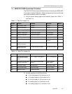
Table 1–1.Two Pin Jumper List
Jumper Function Installed Removed Default
W10 External REFT feed External Internal Removed
W11 External REFB feed External Internal Removed
R39 Positive analog input Transformer coupled No connection Installed
R37 Negative analog input Transformer coupled No connection Installed
R38 Positive analog input Differential amplifier No connection Removed
R36 Negative analog input Differential amplifier No connection Removed
R43, R44 Output clock option ADC clock at output connector Buff clock at output
connector
Removed
R42 Optional output clock
parallel termination
Provides pullup termination No pullup termination Removed
R14 Optional ADC clock
parallel termination
Provides pullup termination No pullup termination Removed
Table 1–2.Three Pin Jumper List
Jumper Function Location: Pins 1–2 Location: Pins 2–3
Default
W1 Band gap input voltage
(power down reference
mode)
REFT voltage to bandgap pin 1.25 V to bandgap pin Removed
W3 Transformer and diff amp
common mode select
ADC output common mode
voltage
External common
mode voltage
1–2
W4 Power down select Operate mode Power down mode 1–2
W5 Output enable select Data bus tristate Data bus enable 2–3
W6 Reference select External reference Internal reference 2–3
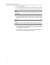
2) Connect supplies to the EVM as follows:
J 1.8-V analog supply to J6 and return to J5
J 1.8-V digital supply to J9 and return to J10
J 3.3-V driver supply to J13 and return to J14
J 5-V analog supply to J7 and return to J8
J –5-V analog supply to J11 and return to J8


