Circuit Function
3-2
3.1 Circuit Function
The following paragraphs describe the function of the individual circuits. See
the data sheet for device operating characteristics.
3.1.1 Analog Inputs
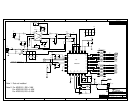
The ADC has either transformer-coupled inputs or differential-amplifier inputs
from a single-ended source. The inputs are provided via the SMA connectors
J1 and J2 on the EVM, which must be configured as follows:
- For a differential amplifier input to the ADC, a single ended source is
connected to J1. R36 and R38 must be installed, and R37 and R39 must
be removed. The input has a 50-Ω terminator.
- For a 1:1 transformer coupled input to the ADC, a single ended source is
connected to J2. R36 and R38 must be removed, and R37 and R39 must
be installed. The input is ac-coupled and has a 50-Ω terminator.
3.1.2 External Reference Inputs
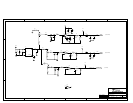
In addition to being able to use the internal reference of the ADC, a reference
circuit has been included on the EVM. This circuit uses a precision 2.5-V,
low-noise linear regulator as the primary source, and allows adjustment of the
REFT and REFB signals to the ADC using potentiometers R27 and R28,
respectively. A third source, CML, is also generated to provide an adjustable
common mode voltage to be used by the transformer and differential amplifier
during external reference operation. CML is adjusted by potentiometer R29.
In order to use the ADC with external references, install jumpers W10 and
W11, install jumper W3 between pins 2 and 3, jumper W6 between pins 1
and 2, and jumper W1 between pins 1 and 2. If REFT is set to any voltage other
than 1.25 V, jumper W1 must be installed between pins 2 and 3 for optimal ADC
performance. The ranges of the external reference signals are shown in
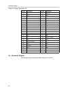
Table 3–1.
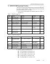
Table 3–1.Reference Voltage Adjustment Ranges
Signal Minimum Voltage Typical Voltage Maximum Voltage
REFT 0.9 1.25 1.6
REFB 0.3 0.75 0.9
CML 0.5 1.0 1.25


