


ChipScope PLBv46 IBA (Bus Analyzer) (v1.00a)
DS619 (v1.0) September 17, 2007 www.xilinx.com
Product Specification 2
R
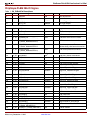
ChipScope PLB46 IBA I/O Signals
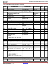
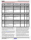
Table 1: IBA_PLBv46 Pin Descriptions
Port MU Signal Name Interface I/O Description
P1 CONTROL ICON I/O Icon control bus IO
P2 PLB_Clk System I System Clock
P3 MU_1C iba_trigin_in GENERIC I Generic Trigger Inputs
P4 iba_trig_out GENERIC O IBA Trigger Output
Reset & Error Status
P5 MU_1A PLB_Rst System I Registered reset output from arbitration
logic
P6 MU_1A Bus_Error_Det System I Bus Error Interrupt
P7 MU_1A PLB_lockErr Slave I PLB lock error indicator
P8 MU_1B PLB_MRdErr[0:
C_PLBV46_NUM_MASTERS-1]
Master I PLB Master slave read error indicator
P9 MU_1B PLB_MWrErr[0:
C_PLBV46_NUM_MASTERS-1]
Master I PLB Master slave write error indicator
P10 MU_1B PLB_MIRQ[0:
C_PLBV46_NUM_MASTERS-1]
Master I Master interrupt request. For each master,
indicates when a slave has encountered an
event that is significant to the master
P11 MU_1B PLB_MTimeout[0:
C_PLBV46_NUM_MASTERS-1]
Master I PLB address-phase timeout indicator
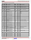
Common Signals
P12 MU_2A PLB_PAValid Slave I PLB primary address valid indicator
P13 MU_2A PLB_SAValid Slave I PLB secondary address
P14 MU_2A PLB_busLock Slave I PLB BusLock
P15 MU_2A PLB_abort Slave I PLB abort bus request indicator
P16 MU_2A PLB_Swait Simulation I Output of Sl_wait OR gate
P17 MU_2A PLB_SaddrAck Simulation I Output of Sl_addrAck OR gate
P18 MU_2A PLB_Srearbitrate Simulation I Output of Sl_rearbitrate OR gate
P19 MU_2A PLB_RNW Slave I PLB read not write
P20 MU_2A PLB_SwrDAck Simulation I Output of Sl_wrDAck OR gate
P21 MU_2A PLB_SwrComp Simulation I Output of Sl_wrComp OR gate
P22 MU_2A PLB_SwrBTerm Simulation I Output of Sl_wrBTerm OR gate
P23 MU_2A PLB_wrBurst Slave I PLB burst write transfer indicator
P24 MU_2A PLB_SrdDAck Simulation I Output of Sl_rdDAck OR gate
P25 MU_2A PLB_SrdComp Simulation I Output of Sl_rdComp OR gate
P26 MU_2A PLB_SrdBTerm Simulation I Output of Sl_rdBTerm OR gate
P27 MU_2A PLB_rdBurst Slave I PLB burst read transfer indicator
P28 MU_2B PLB_size[0:3] Slave I PLB Transfer size
P29 MU_2B PLB_type[0:2] Slave I PLB Transfer type
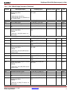
P30 MU_2B PLB_MSize[0:1] Slave I PLB data bus port width indicator.
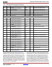
P31 MU_2B PLB_Ssize[0:1] Simulation I Output of slave Sl_SSize OR gate
P32 MU_2B PLB_masterID[0:
C_PLBV46_MID_WIDTH-1]
Slave I PLB current master identifier
P33 MU_2B PLB_BE[0: C_PLBV46_DWIDTH/8-1] Slave I PLB byte enables