


ZXLD1362EV3 User Guide issue 1 3/7 11-01-2008
ZXLD1362EV3 EVALUATION BOARD
REFERENCE DESIGN
The ZXLD1362EV3 is configured to the reference design in Figure 2. The target application is a driver for one or
more series-connected LEDs for luminaires in both commercial and automotive applications.
The maximum operating voltage is 60V, and the nominal current is set at 700mA with a
0.15Ω sense resistor R1. The
device operates in continuous mode at approximately 150 kHz, with a 68uH inductor.
An accurate way of determining the current, avoiding the need to insert an ammeter in the current path, is to measure
the voltage on the sense resistor. A 10K resistor and a 1uF capacitor can be used to form a low pass filter and the
voltage across the capacitor represents a more stable dc reading of current. Using this method, 100mV represents
0.7 Amp when using a 0.15 sense resistor.
The ADJ pin connects to a low pass filter within the ZXLD1362 chip to provide some decoupling, but the external
capacitor C2 (100nF) is used to provide additional decoupling to reduce any high frequency noise as well as
enabling the soft start function.
Both DC and PWM dimming can be achieved by driving the ADJ pin. For DC dimming, the ADJ pin may be driven
between 0.3V and 1.25V. Driving the ADJ pin below 0.2V will shut down the output current. For PWM dimming, an
external open-collector NPN transistor or open-drain N-channel MOSFET can be used to drive the ADJ pin. The
PWM frequency can be low, around 100Hz to 1 kHz, or high between 10 kHz to 50 kHz.
For low frequency, PWM capacitor C2 should be removed on the evaluation board, to give a more accurate duty
cycle.
Shorting R2 will connect the test pin ADJ to device pin ADJ if needed.
The external capacitor C2 on the ADJ pin sets the soft start time. The amount of soft start time achievable is
approximately 0.2ms/nF.
For other reference designs or further applications information, please refer to the ZXLD1362 datasheet.
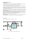
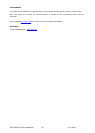
Schematic Diagram
Figure 2 shows the schematic for the ZXLD1362EV3 evaluation board.
Figure 2: Schematic for the evaluation board ZXLD1362EV3
ZXLD1362
GND
ADJ LX
Vin V sense
R1
R2
C4
C2
C1
L1
D1
C3
Vin
LED
K
ADJ
LED
A
1
54
3
GND