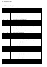
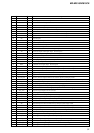
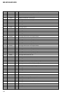
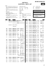
MZ-NF810/NF810CK
3838
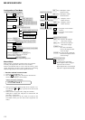
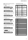
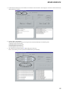
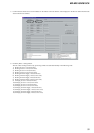
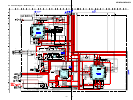
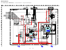
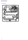
Note on Schematic Diagram:
• All capacitors are in µF unless otherwise noted. pF: µµF
50 WV or less are not indicated except for electrolytics
and tantalums.
• All resistors are in Ω and
1
/
4
W or less unless otherwise
specified.
•%: indicates tolerance.
•
f
: internal component.
• C : panel designation.
• A : B+ Line.
•Total current is measured with MD installed.
•Power voltage is dc 3 V and fed with regulated dc power
supply from DC IN 3 V jack (J951).
•Voltages and waveforms are dc with respect to ground in
playback mode.
no mark : PLAYBACK
(): REC
∗
: Impossible to measure
•Voltages are taken with a VOM (Input impedance 10 MΩ).
Voltage variations may be noted due to normal produc-
tion tolerances.
•Waveforms are taken with a oscilloscope.
Voltage variations may be noted due to normal produc-
tion tolerances.
• Circled numbers refer to waveforms.
• Signal path.
J : PLAYBACK
c : DIGITAL IN
F : ANALOG IN
f : RECORD
N : USB
• The voltage and waveform of CSP (chip size package)
cannot be measured, because its lead layout is different
form that of conventional IC.
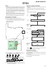
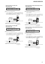
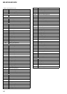
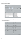
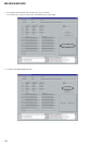
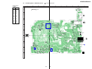
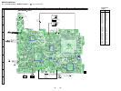
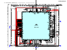
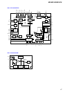
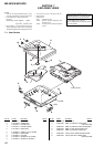
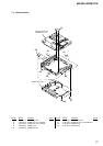
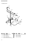
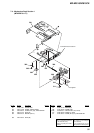
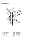
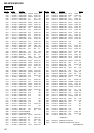
6-2. Note For Printed Wiring Board And Schematic Diagrams
Note on Printed Wiring Board:
• X : parts extracted from the component side.
• Y : parts extracted from the conductor side.
• : Pattern from the side which enables seeing.
(The other layers' patterns are not indicated.)
Caution:
Pattern face side: Parts on the pattern face side seen from
(Conductor Side) the pattern face are indicated.
Parts face side: Parts on the parts face side seen from
(Component Side) the parts face are indicated.
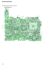
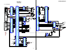
• MAIN board is four-layer printed board.
However, the patterns of layers 2 and 3 have not been
included in this diagrams.
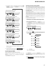
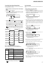
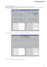
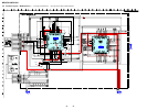
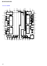
• Lead Layouts
surfac
Lead layout of conventional IC CSP (chip size package)
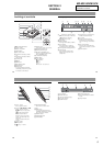
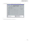
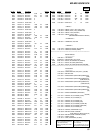
5 IC801 2 (OSCO)
(at the point of R806)
44.3ns
2 IC501 rd (TE)(SL501)
500mV/DIV, 1ms/DIV
7 IC901 yd (CLK)
6 IC801 <z,/ (UOSCO)
(USB mode)
(at the point of R823)
3 IC501 rs (FE)(SL502)
1 IC501 9 (RFO)(TP1517)
500mV/DIV, 200ns/DIV
4 IC601 4 (CLK)
1V/DIV, 2
µ
s/DIV
5.67
µ
s
8 IC301 9 (MCLK)
2Vp-p
780mVp-p
1.2Vp-p
2.4Vp-p
2.6Vp-p
1V/DIV, 40ns/DIV
88.6ns
9 IC301 8 (BCLK)
(REC mode)
1V/DIV, 100ns/DIV
354ns
0 IC301 q; (LRCK)
(REC mode)
22.7
µ
s
2.6Vp-p
2.4Vp-p
1V/DIV, 10
µ
s/DIV
20.8ns
3.2Vp-p
1V/DIV, 2
µ
s/DIV
5.67
µ
s
2.4Vp-p
200mV/DIV, 1ms/DIV
240mVp-p
500mV/DIV, 20ns/DIV
1V/DIV, 10ns/DIV
•Waveforms
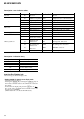
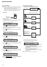
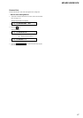
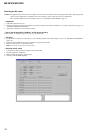
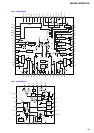
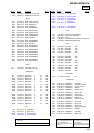
* Replacement of IC501,IC801 on MAIN board requires a
special tool.
* Replacement of IC501,IC801 on MAIN board requires a
special tool.
✩When IC851 is damaged, replace the MAIN board.
✩When IC851 is damaged, replace the MAIN board.
Note:
The components identified by
mark 0 or dotted line with mark
0 are critical for safety.
Replace only with part number
specified.
Note:
Les composants identifiés par
une marque 0 sont critiques
pour la sécurité.
Ne les remplacer que par une
pièce portant le numéro spécifié.
•Abbreviation
3CED : Spanish, Swedish, Portuguese and Finnish model
4CED : French, German, Dutch and Italian model