


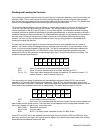
Enabling/Disabling I/O Buffers
When using the tristate mode (Jumper in the TST position), the method to disable the I/O buffers involved
writing a control word to the Control Register at Base Address +3. This control word was required to have
bit D7 (the most significant bit) set. That meant that the PPI translated it as an "active mode set" and reset
the output data latches to "zero" on all output ports and the output buffers were disabled. However, if the
buffers are to be enabled at a later time, the output latches will be in a "zero" state. For example, if all the
outputs were 1's, they will now be 0's and the output buffers will be disabled. This problem can be
resolved as follows.
Two computer I/O bus addresses are available that permit you to enable or disable the I/O buffers at will,
without programming the PPI mode. Buffers are enabled/disabled at Base Address + C. To enable the
buffers and to set outputs to the desired state, you can write to Base + C with bit D7 low. If you wish to
subsequently disable the buffers, you can write to Base + C with bit D7 high. In this way you can
enable/disable the output buffers without programming the PPI mode.
Note
When writing a command byte to the card while the TST jumper is installed, the PPI output buffers are
disabled. Thus, when you desire to to change the mode, you must first set the new mode and then enable
the buffers. Enabling the buffers can be done at either Base Address +3 or Base Address +A.
Interrupts
The card has three sources of interrupts:
1.
A Digital I/O signal on Pin 9 for the H version (50 pin), or Pin 7 for the D version (37 pin).
The Digital I/O interrupt is Port C bit 3 and is enabled by installing jumpers IRQD and
INT. Port C bit 3, if set for an output, can be toggled under program control to generate
an interrupt.
2. An External TTL input signal on Pin 22 for the H version only. This interrupt is enabled by
installing jumpers IRQD and EXT. The H version of the card also has an active-low input
to disable interrupts on J1 pin 20.
3. An onboard Timer output signal from the first 82C54 output 2 (S01, S02, and S03
versions only). The Timer interrupt is enabled by installing jumpers IRQT and INT. This
feature allows a “clock tick interrupt”.
All interrupts are triggered on the rising edge of the signal source.
All interrupts are enabled through software by writing any value to Base+E, and disabled through software
by writing any value to Base+D.
All interrupts are cleared by writing any value to Base+F.
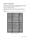
Refer to Chapter 3 for hardware enabling and disabling of interrupts. Refer to Table 6-1 for more on
software control.
Manual PCI-DIO-24DH
20