


Z8F04A08100KIT Development Kit
User Manual
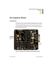
Development Board UM018702-0505
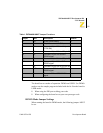
12
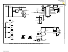
J3 1-2
J4 OUT
J5 1-2
J6 1-2
J7 OUT
J8 1-2
J9 1-2
J10 1-2
J11 OUT
USER DEBUG Mode Jumper Settings
When running the board in USER DEBUG mode, the following jumpers
MUST be set:
J3 OUT
J4 IN
J6 OUT
J7 IN
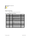
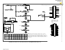
Switches S1, S2, and SW1
Switches S1, S2, and SW1 on the Z8 Encore! XP™ 4K Series 8-Pin
Development board perform the following functions:
•
S1 – Test switch
•
S2 – Power ON/OFF switch
•
SW1 – RESET
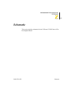
External Interface Headers JP1 and JP2
External interface headers JP1 and JP2 are shown in the schematic on
page 15.