


UM018702-0505
Z8F04A08100KIT
User Manual
18
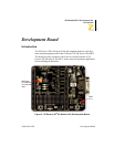
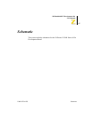
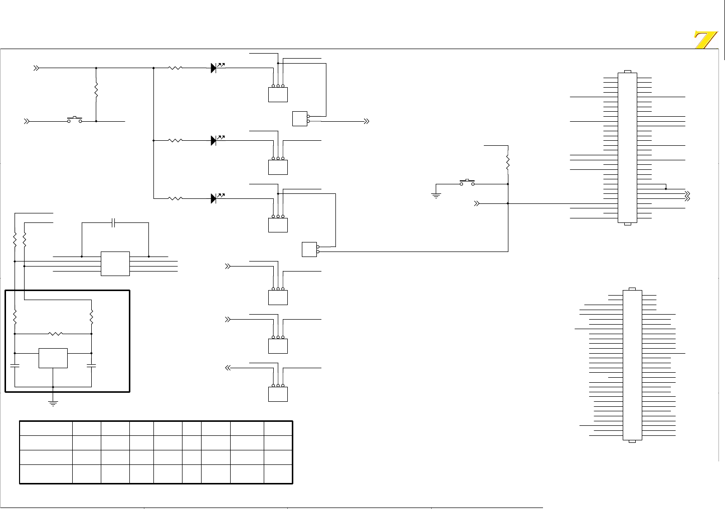
Schematic, Z8 Encore! XP™ 4K Series 8-Pin MCU Development Board, Page 2 of 2
connecto
r 2
Connector
JP1
for referen
ce
only
Note
1:
If Module is plugged onto the De
v Platform the local
RS232 interface is disabled
by pin 50 of JP2
8 pin foot
print
RESET
NOTE
2
Note 2:
The XP supports internal oscillator, extern
al crystal, or ceramic
resonator, external R/C and external CMOS dr
ive clock modes. R16,
R17, R19, R20, R21, C10, C11 and Y1 are used to
support the clock mode
selected. The development board is shipped c
onfigured for internal
oscillator. When using internal oscilator, p
ins 2 and 3 could be used
as GPIO ports PA0 and PA1. Table 1 shows th
e recommended clock mode
configurati
ons.
Clock Mode R16 R17 R19 R20
R21 C10 C11 Y1
Internal Note 2 Note 2 none none no
ne none none none
Ceramic Res none none 0 Ohm 0 Ohm 22
0K 10-20pF 10-20pF user
select
Crystal none none 0 Ohm 0 Ohm 22
0K 10-20 pF 10-20 pF user
select
TABLE
1
TES
T
PA0
DEMO USER
PA1
PA2
DEMO USER
DEMO USER
PA3
PA4
PA5
DEMO USER
DEMO USER
USERDEMO
RESET
96C
0964-001
B
XP 4K 8pin
MDS Processor Module. Schematic.
B
22
Tuesday, December 14, 2004
Title
Siz
e
Document Number
Rev
Date:
Sheet
of
A20
-CS0
A12
-IOREQ
-F91_WE
A13
GND
GND
A17
A21
VCC_33V
A14
D1
VCC_33V
D7
-DIS_FLASH
GND
A6 A0
D3
D6
-BUSACK
A3
D2
VCC_33V
A15
A4
-TRS
TN
D0
-MREQ
A7
A10
A9
A16A18
A11
-INSTRD
A19
A5
GND
D5
-CS1
A22
A1A2
-CS2
-RD
A8
GND
D4
A23
-WR
-BUSREQ
GND
PA3_MDS
VCC_33V
PA2_MDS
PA1_MDS
GND
GND
PA4_MDS PA5_MDS
GND
GND
PA0_MDS
GND
VCC_33V
-DIS_IrDA
PA2_JP
GND
PA5_JP
PA3_JP
PA4_JP
PA0
PA1
GND
VCC_33V
PA0_JP
PA1_JP
PA0_JP
PA1_JP
PA2_JP
PA3_JP
PA4_JP
PA5_JP
PA5_T
XD0
PA4_RXD
0
PA3_CTS
0
LED_R
LED_G
PA0_MDS
PA1_MDS
PA2_MDS
PA3_MDS
PA4_MDS
PA5_MDS
VCC_33VVCC_33VVCC_33VVCC_33VVCC_33VVCC_33V
PA3_CTS
0
-RESE
T
-RESE
T
VCC_33V
DBG
LED_Y
VCC_33V
GND
VCC_33V
-DIS_IRDA
-DIS_232
PA5_TX
D0
PA3_CTS
0
PA4_RXD
0
-RESET
DBG
J6
Header 3
1
2
3
U5
Z8F04xA_8pin
4
3
2 7
6
5
81
PA2
PA1
PA0 PA5
PA4
PA3
VSS
VDD
R19
0
SW1
J5
Header 3
1
2
3
C11
R20
0
J10
Header 3
1
2
3
D4
LED
RED
2 1
R15
10
0
J3
Header 3
1
2
3
D3
LED
YEL
2 1
C13
Y1
20 MHz
1
2
3
1
2
3
D2
LED
GREEN
2 1
S1
1 2
R13
10
0
J9
Header 3
1
2
3
J7
HEADER 2
1
2
R21
220K
R16
0
R11
10
0
C10
J4
HEADER 2
1
2
JP2
HEADER 30x2/SM
2
4
6
8
10
12
14
16
18
20
22
24
26
28
30
32
34
36
38
40
42
44
46
48
50
52
54
56
58
60
1
3
5
7
9
11
13
15
17
19
21
23
25
27
29
31
33
35
37
39
41
43
45
47
49
51
53
55
57
59
J8
Header 3
1
2
3
R14
10K
R12
10K
R17
0
JP1
HEADER 30x2/SM
2
4
6
8
10
12
14
16
18
20
22
24
26
28
30
32
34
36
38
40
42
44
46
48
50
52
54
56
58
60
1
3
5
7
9
11
13
15
17
19
21
23
25
27
29
31
33
35
37
39
41
43
45
47
49
51
53
55
57
59