


30 Electrical Data Chapter 8
AMD Athlon™ XP Processor Model 10 Data Sheet 26237C—May 2003
Preliminary Information
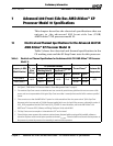
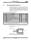
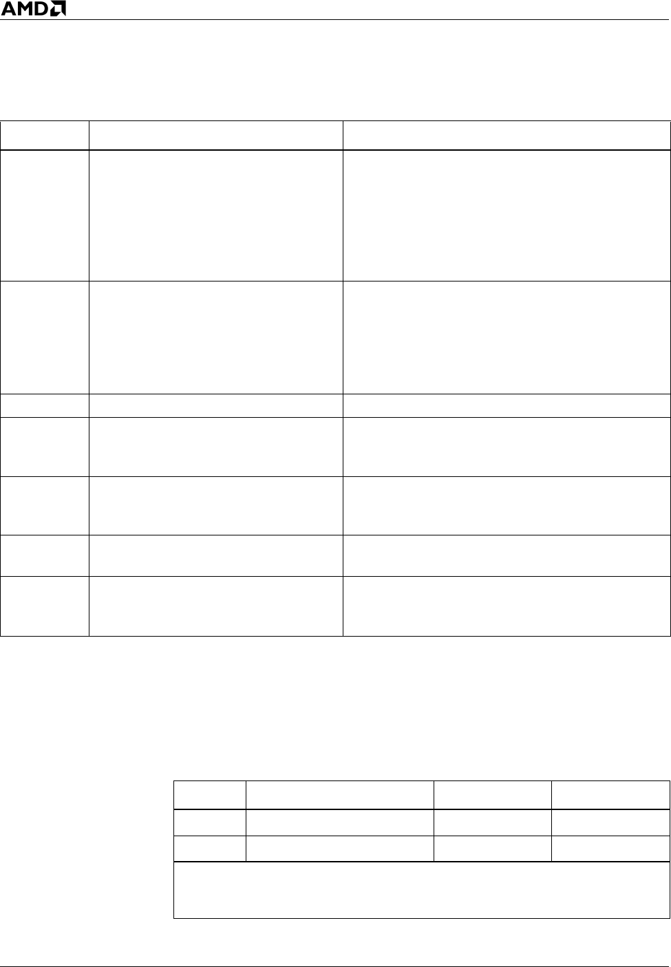
8.3 Voltage Identification (VID[4:0])
Table 10 shows the VID[4:0] DC Characteristics. For more infor-
mation on VID[4:0] DC Characteristics, see “VID[4:0] Pins” on
page 77.
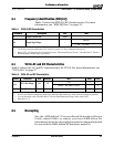
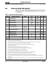
AMD Athlon™
System Bus
SADDIN[14:2]#, SADDOUT[14:2]#,
SADDINCLK#, SADDOUTCLK#, SFILLVAL#,
SDATAINVAL#, SDATAOUTVAL#,
SDATA[63:0]#, SDATAINCLK[3:0]#,
SDATAOUTCLK[3:0]#, CLKFWDRST,
PROCRDY, CONNECT
See “Advanced 333 FSB AMD Athlon™ System Bus DC
Characteristics” on page 24, See “Advanced 400 FSB
AMD Athlon™ System Bus DC Characteristics” on page
28, Table 3, “Advanced 333 FSB AMD Athlon™ System
Bus AC Characteristics,” on page 23, Table 7, “Advanced
400 FSB AMD Athlon™ System Bus AC Characteristics,”
on page 27, and “CLKFWDRST Pin” on page 72.
Southbridge
RESET#, INTR, NMI, SMI#, INIT#, A20M#,
FERR, IGNNE#, STPCLK#, FLUSH#
See “General AC and DC Characteristics” on page 36,
“INTR Pin” on page 76, “NMI Pin” on page 76, “SMI#
Pin” on page 77, “INIT# Pin” on page 75, “A20M# Pin”
on page 72, “FERR Pin” on page 73,“IGNNE# Pin” on
page 75, “STPCLK# Pin” on page 77, and “FLUSH# Pin”
on page 75.
JTAG TMS, TCK, TRST#, TDI, TDO See “General AC and DC Characteristics” on page 36.
Test
PLLBYPASS#, PLLTEST#, PLLMON1,
PLLMON2, SCANCLK1, SCANCLK2,
SCANSHIFTEN, SCANINTEVAL, ANALOG
See “General AC and DC Characteristics” on page 36,
“PLL Bypass and Test Pins” on page 76, “Scan Pins” on
page 77, “Analog Pin” on page 72.
Miscellaneous DBREQ#, DBRDY, PWROK
See “General AC and DC Characteristics” on page 36,
“DBRDY and DBREQ# Pins” on page 73, “PWROK Pin”
on page 76.
APIC PICD[1:0]#, PICCLK
See “APIC Pins AC and DC Characteristics” on page 41,
and “APIC Pins, PICCLK, PICD[1:0]#” on page 72.
Thermal THERMDA, THERMDC
See Table 17, “Thermal Diode Electrical Characteristics,”
on page 39, and “THERMDA and THERMDC Pins” on
page 77.
Table 9. Interface Signal Groupings (continued)
Signal Group Signals Notes
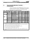
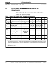
Table 10. VID[4:0] DC Characteristics
Parameter Description Min Max
I
OL
Output Current Low 6 mA
V
OH
Output High Voltage – 5.25 V *
Note:
* The VID pins are either open circuit or pulled to ground. It is recommended that these pins
are not pulled above 5.25 V, which is 5.0 V + 5%.