


Chapter 11 Pin Descriptions 75
26237C—May 2003 AMD Athlon™ XP Processor Model 10 Data Sheet
Preliminary Information
signals High above 2.5 V. Do not expose these pins to a
differential voltage greater than 1.60 V, relative to the
processor core voltage.
Refer to “VCC_2.5V Generation Circuit” found in the section,
“Motherboard Required Circuits,” of the AMD Athlon™
Processor Motherboard Design Guide, order# 24363 for the
required supporting circuitry.
See “Frequency Identification (FID[3:0])” on page 25 for the
DC characteristics for FID[3:0].
FSB_Sense[1:0] Pins FSB_Sense[1:0] pins are either open circuit (logic level of 1) or
are pulled to ground (logic level of 0) on the processor package
with a 1 kΩ resistor. In conjunction with a circuit on the
motherboard, these pins may be used to automatically detect
the front-side bus (FSB) setting of this processor. Proper
detection of the FSB setting requires the implementation of a
pull-up resistor on the motherboard. Refer to the AMD Athlon™
Processor-Based Motherboard Design Guide, order# 24363 and the
technical note FSB_Sense Auto Detection Circuitry for Desktop
Processors, order# TN26673 for more information.
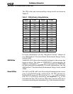
Table 26 is the truth table to determine the FSB of desktop
processors.
The FSB_Sense[1:0] pins are 3.3-V tolerant.
FLUSH# Pin FLUSH# must be tied to V
CC_CORE
with a pullup resistor. If a
debug connector is implemented, FLUSH# is routed to the
debug connector.
IGNNE# Pin IGNNE# is an input from the system that tells the processor to
ignore numeric errors.
INIT# Pin INIT# is an input from the system that resets the integer
registers without affecting the floating-point registers or the
internal caches. Execution starts at 0_FFFF_FFF0h.
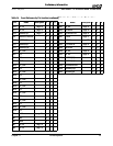
Table 26. Front-Side Bus Sense Truth Table
FSB_Sense[1] FSB_Sense[0] Bus Frequency
1 0 RESERVED
11133 MHz
01166 MHz
0 0 200 MHz